Verilog code for 2:1 Multiplexer (MUX) – All modeling styles
- Gate level modeling
- Dataflow modeling
- Behavioral modeling
- Structural modeling
In this article, we’ll write the Verilog code for the simplest multiplexer, i.e. a 2:1 MUX.
Comparing 2:1 with 2^n: 1 (as mentioned before) we get n = 1, which is the number of select lines (input variables = 2, select lines = 1, output signal = 1). Now before jumping to the coding section, a brief description of each modeling style has been presented before you.
Gate Level Modeling
As the name suggests, this style of modeling will include primitive gates that are predefined in Verilog. This is virtually the lowest abstraction layer, which is used by designers for implementing the lowest level modules, as the switch level modeling isn’t that common. The prerequisite for this style is knowing the basic logic diagram of the digital circuit that you wish to code.
Since we’re concerned about designing the Verilog code for a 2:1 MUX, have a look at its circuit diagram.
Logic circuit
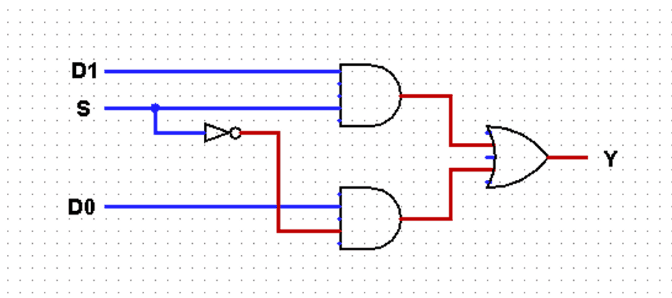
The input signals are
D0 and D1. S is the select line with Y as its output. We can orally solve for the expression of the output that comes out to be:
Y = D0.S’ + D1.S
Verilog code for 2:1 MUX using gate-level modeling
For the gate level, we will first declare the module for 2: 1 MUX, followed by the input-output signals. The order of mentioning output and input variables is crucial here, the output variable is written first in the bracket, then the input ones.
module m21(Y, D0, D1, S);
The
module is a keyword here. m21 is the name of the module. Y is the output and D0, D1 and S being input are written after. Note that we don’t declare intermediate signals while defining the module.
Next comes the declaration of input, output, and intermediate signals. You might have noticed that other modeling styles include the declaration of variables along-with their respective data- types. But in the gate- level, we only declare the intermediate variables as wire; there’s no need for
reg or wire declaration for input-output entities.output Y; input D0, D1, S; wire T1, T2, Sbar;
Next comes the instantiation part for gates.
and not and or are the predefined built-in gates, and we’re instantiating these gates with their respective input-output ports.
For example for
not gate, Sbar is the output and S is the input. Similarly for and gate, T1, D1, and T2, D2 are inputs to two and gates and S and Sbar are their respective output.and (T1, D1, S), (T2, D0, Sbar); not (Sbar, S); or (Y, T1, T2);
The
endmodule marks the end of the module.endmodule
Here’s the final code of the 2:1 mux using gate-level modeling.
module m21(Y, D0, D1, S);

output Y;
input D0, D1, S;
wire T1, T2, Sbar;

and (T1, D1, S), (T2, D0, Sbar);
not (Sbar, S);
or (Y, T1, T2);

endmodule
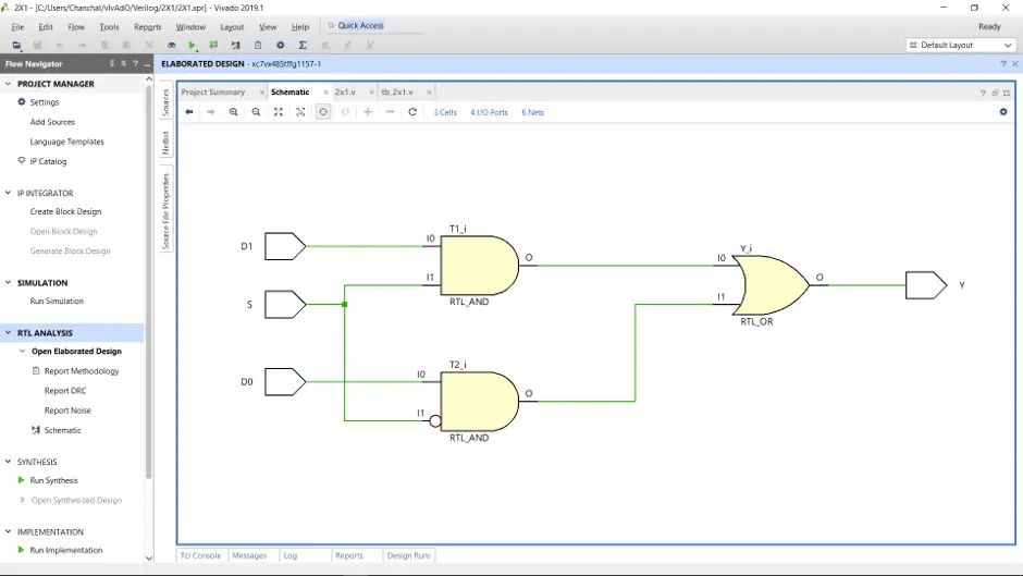
RTL Schematic
This is the design abstraction, which shows the internal circuitry involved. It is the hardware implementation of a system.
Data flow modeling
The dataflow level shows the nature of the flow of data in continuous assignment statements (
assign keyword). It describes the combinational circuit by their functions rather than their gate structures. For coding in the dataflow style, we only need to know about the logical expression of the circuit.Logical Expression
The equation for 2:1 mux is:
Y = D0.S’ + D1.S
where Y is the final output, D0, D1, and S are inputs.
Verilog code for 2:1 MUX using data flow modeling
To start with this, first, you need to declare the module. There’s no need for data- type declaration in this modeling.
module m21(Y, D0, D1, S);
output Y;
input D0, D1, S;
Now since this the dataflow style, one is supposed to use
assign statements. I have used a ternary operator for the output Y. This operator ? means that the output Y becomes equal to data D1 if select line S is true otherwise D0 is the final output.assign Y= (S)? D1: D0;
Final code:
module m21(D0, D1, S, Y);

output Y;
input D0, D1, S;

assign Y=(S)?D1:D0;

endmodule
RTL Schematic
The hardware schematic for a 2:1 multiplexer in dataflow level modeling is shown below. You will notice that this schematic is different from that of the gate-level. It involves the symbol of a multiplexer rather than showing up the logic gates involved, unlike gate-level modeling.

Behavioral modeling
This level describes the behavior of a digital system. In most of the cases, we code the behavioral model using the truth table of the circuit.
Truth-table for 2:1 MUX
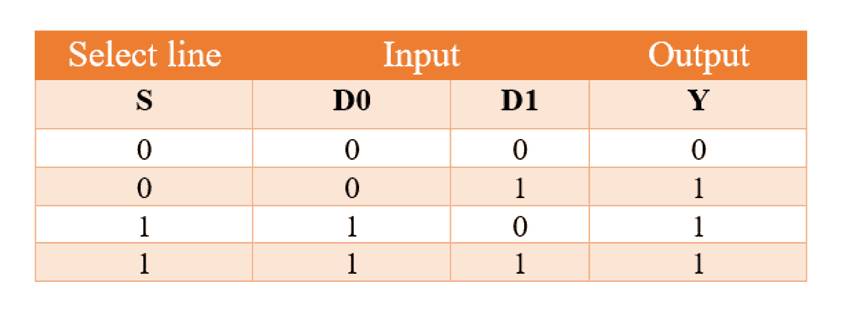
Now to find the expression, we will use K- map for final output
Y.
Equation from the truth table: Y = D0.S’ + D1.S
Verilog code for 2:1 MUX using behavioral modeling
First, define the
module m21 and declare the input and output variables.module m21( D0, D1, S, Y);
Don’t forget to mention the data- type of the ports. Since it is the behavioral modeling, we will declare the output
Y as reg while the rest of the inputs as wire.input wire D0, D1, S; output reg Y;
Behavioral modeling mainly includes two statements:
- An
initialstatement which is executed the only once alwaysstatement, which is executed once the sensitivity list is activated.
You should notice that the output is equal to the second input if the select line is high. Otherwise, it is equal to the first input itself. This logic can be stated by using the
if-else statement.
Since the output of 2:1 MUX changes once there is a change in
D0 OR D1 OR S we’ll use always statement. Now, if the S event is true, the output Y will be D1, else the output will be D0.always @(D0 or D1 or S) begin if(S) Y= D1; else Y=D0; end
Summing up the final code:
module m21( D0, D1, S, Y);
input wire D0, D1, S;
output reg Y;

always @(D0 or D1 or S)
begin

if(S)
Y= D1;
else
Y=D0;

end

endmodule
RTL Schematic
Hardware schematic for 2:1 MUX:
Structural modeling
Structural modeling describes the hardware structure of a digital system. It is usually written in RTL and is somewhat similar to gate-level modeling. The only difference is it doesn’t include any built-in gates. The components and connections all need to separately defined here. There’s a proper definition for the expression of the digital system within the module itself. It includes module declaration and instantiation, port-list and it’s associates.
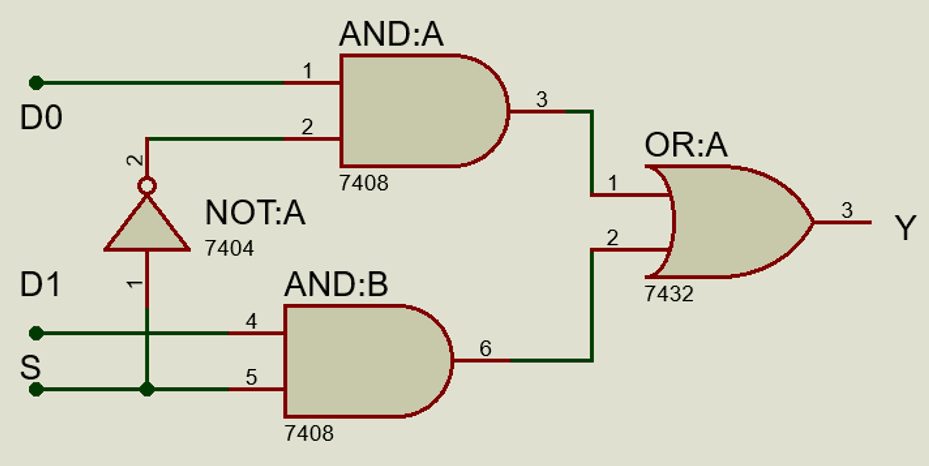
Logic circuit
Now the logical diagram for a 2:1 MUX shows that we need two AND gates, one OR gate and one NOT gate. We’ll structurize for each of the gates separately.

Verilog code for 2:1 MUX using structural modeling
First, we’ll start by declaring the modules for each logic gate. Below is the declaration of a module for AND gate, we can define the input-output variables in the next line also. We don’t need the data- type for signals since it’s the structure of the circuit that needs to be emphasized.
module and_gate(output a, input b, c);
Now using the
assign statement, write the function of the logic gate in a statement. You may use the delay.assign a = b & c; endmodule
That marks the end of a module for AND gate. Similarly for other gates also:
NOT gate =>
module not_gate(output d, input e);
assign d = ~ e;
endmodule
OR gate =>
module or_gate(output l, input m, n);
assign l = m | n;
endmodule
NOTE: use a different variable name for each input and output signal.
Time for us to combine these individual modules for logic gates into one single module for 2:1 MUX. This is done with the help of a concept called module instantiation and falls under a separate module top. The above individual modules will be used in the following by instantiating them with the name_of_the_instance. Instantiation is used when we want to repeat a particular function/ module for different sets of input.
First, write the name of the module you need. Then give the instance a name. The association list will contain the output signal first, followed by the input ones.
and_gate u1(T1, D1, S);
Here and_gate is the name of the module,
u1 is the instance’s name. T1 wire(which is the intermediate signal) is the output, D1 and S are input. Repeat this for the rest of the modules after considering the logic diagram.and_gate u1(T1, D1, S); not_gate u2(T2, S); and_gate u3(T3, D0, T2); or_gate u4(Y, T1, T3);
Here’s the final code for 2:1 mux in structural style.
module and_gate(output a, input b, c);
assign a = b & c;
endmodule

module not_gate(output d, input e);
assign d = ~ e;
endmodule

module or_gate(output l, input m, n);
assign l = m | n;
endmodule

module m21(Y, D0, D1, S);
output Y;
input D0, D1, S;
wire T1, T2, T3;
and_gate u1(T1, D1, S);
not_gate u2(T2, S);
and_gate u3(T3, D0, T2);
or_gate u4(Y, T1, T3);
endmodule
RTL schematic
Testbench for the 2:1 Mux in Verilog
A testbench drives the input to the design code of the system. It is used to provide the initial stimulus to the input signals and check for the entire range of possible combinations. You may find a detailed explanation and steps to write the testbench over here!
This is the testbench code for the 2:1 multiplexer.
module top;
wire out;
reg d0, d1, s;
m21 name(.Y(out), .D0(d0), .D1(d1), .S(s));
initial
begin
d0=1'b0;
d1=1'b0;
s=1'b0;
#100 $finish;
end
always #40 d0=~d0;
always #20 d1=~d1;
always #10 s=~s;
always@(d0 or d1 or s)
$monitor("At time = %t, Output = %d", $time, out);
endmodule;
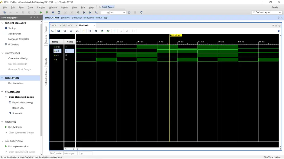
Simulation Waveform
Here is the final simulated waveform for the 2X1 MUX circuit.


沒有留言:
張貼留言