參考來源 https://cerkit.com/2019/09/15/driving-the-max7219-7-segment-display-device-from-a-tinyfpga-using-verilog/
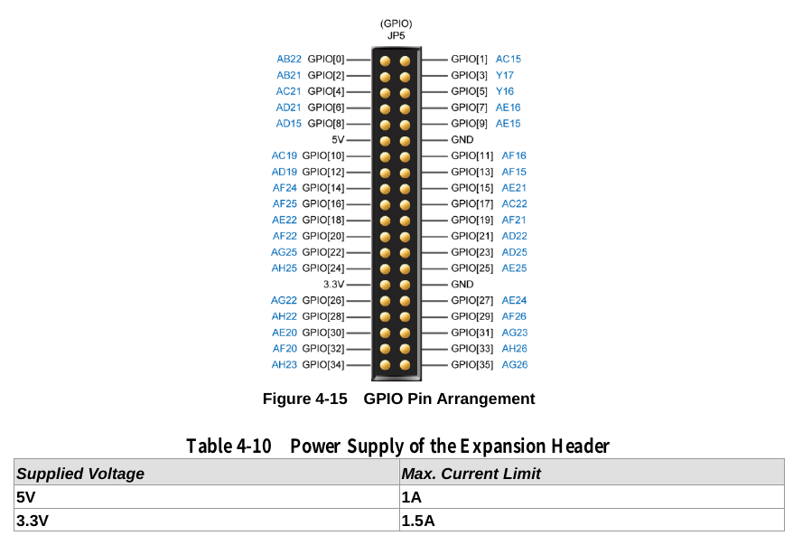
注意: 須將DE2-115 pin assignments 接腳的GPIO
Bidir雙向改成UnKnown
Bidir無法使用
GPIO[15],Bidir,PIN_AE21,4,B4_N1,3.3-V LVTTL,
GPIO[14],Bidir,PIN_AF24,4,B4_N1,3.3-V LVTTL,
GPIO[13],Bidir,PIN_AF15,4,B4_N2,3.3-V LVTTL,
GPIO[12],Bidir,PIN_AD19,4,B4_N0,3.3-V LVTTL,
GPIO[11],Bidir,PIN_AF16,4,B4_N2,3.3-V LVTTL,
GPIO[10],Bidir,PIN_AC19,4,B4_N0,3.3-V LVTTL,
GPIO[9],Bidir,PIN_AE15,4,B4_N2,3.3-V LVTTL,
GPIO[8],Unknown,PIN_AD15,4,B4_N2,3.3-V LVTTL,
GPIO[7],Unknown,PIN_AE16,4,B4_N2,3.3-V LVTTL,
GPIO[6],Unknown,PIN_AD21,4,B4_N0,3.3-V LVTTL,
GPIO[5],Unknown,PIN_Y16,4,B4_N0,3.3-V LVTTL,
GPIO[4],Unknown,PIN_AC21,4,B4_N0,3.3-V LVTTL,
GPIO[3],Unknown,PIN_Y17,4,B4_N0,3.3-V LVTTL,
GPIO[2],Unknown,PIN_AB21,4,B4_N0,3.3-V LVTTL,
GPIO[1],Unknown,PIN_AC15,4,B4_N2,3.3-V LVTTL,
GPIO[0],Unknown,PIN_AB22,4,B4_N0,3.3-V LVTTL,


//=================================
// look in pins.pcf for all the pin names on the TinyFPGA BX board
module MAX_7219(GPIO ,SW, LEDR, LEDG , CLOCK_50 ,KEY );
input [17:0] SW; // toggle switches
input [7:0] KEY; // Push bottom
input CLOCK_50; //Clock 50Mhz
output [17:0] LEDR; // red LEDS
output [7:0] LEDG; // green LEDs
output [35:0]GPIO;
wire CLK;
Clock_divider (CLOCK_50,CLK); // 16MHz clock
reg PIN_13; // Max7219 CLK
reg PIN_12; // Max7219 DIN;
reg PIN_11; // Max7219 CS
assign GPIO[0]=PIN_13;
assign GPIO[1]=PIN_12;
assign GPIO[2]=PIN_11;
////////
// Display DEADBEEF on 7-Segment Display
////////
//reg rst;
//assign rst = SW[0];
reg rst = 1'b1;
wire M_max_cs;
wire M_max_dout;
wire M_max_sck;
wire M_max_busy;
reg [7:0] M_max_addr_in;
reg [7:0] M_max_din;
reg M_max_start;
max7219 max (
.clk(CLK),
.rst(rst),
.addr_in(M_max_addr_in),
.din(M_max_din),
.start(M_max_start),
.cs(M_max_cs),
.dout(M_max_dout),
.sck(M_max_sck),
.busy(M_max_busy)
);
localparam IDLE_state = 3'd0;
localparam SEND_RESET_state = 3'd1;
localparam SEND_MAX_INTENSITY_state = 3'd2;
localparam SEND_NO_DECODE_state = 3'd3;
localparam SEND_ALL_DIGITS_state = 3'd4;
localparam SEND_WORD_state = 3'd5;
localparam HALT_state = 3'd6;
reg [2:0] M_state_d, M_state_q = IDLE_state;
reg [63:0] M_segments_d, M_segments_q = 1'h0;
reg [2:0] M_segment_index_d, M_segment_index_q = 1'h0;
reg [7:0] max_addr;
reg [7:0] max_data;
// Define the Characters used for display
localparam C0 = 8'h7e;
localparam C1 = 8'h30;
localparam C2 = 8'h6d;
localparam C3 = 8'h79;
localparam C4 = 8'h33;
localparam C5 = 8'h5b;
localparam C6 = 8'h5f;
localparam C7 = 8'h70;
localparam C8 = 8'h7f;
localparam C9 = 8'h7b;
localparam A = 8'h77;
localparam B = 8'h1f;
localparam C = 8'h4e;
localparam D = 8'h3d;
localparam E = 8'h4f;
localparam F = 8'h47;
localparam O = 8'h1d;
localparam R = 8'h05;
localparam MINUS = 8'h40;
localparam BLANK = 8'h00;
always @* begin
M_state_d = M_state_q;
M_segments_d = M_segments_q;
M_segment_index_d = M_segment_index_q;
M_segments_d[56+7-:8] = D;
M_segments_d[48+7-:8] = E;
M_segments_d[40+7-:8] = A;
M_segments_d[32+7-:8] = D;
M_segments_d[24+7-:8] = B;
M_segments_d[16+7-:8] = E;
M_segments_d[8+7-:8] = E;
M_segments_d[0+7-:8] = F;
max_addr = 8'h00;
max_data = 8'h00;
M_max_start = 1'h0;
case (M_state_q)
IDLE_state: begin
rst <= 1'b0;
M_segment_index_d = 1'h0;
M_state_d = SEND_RESET_state;
end
SEND_RESET_state: begin
M_max_start = 1'h1;
max_addr = 8'h0c;
max_data = 8'h01;
if (M_max_busy != 1'h1) begin
M_state_d = SEND_MAX_INTENSITY_state;
end
end
SEND_MAX_INTENSITY_state: begin
M_max_start = 1'h1;
max_addr = 8'h0a;
max_data = 8'hFF;
if (M_max_busy != 1'h1) begin
M_state_d = SEND_NO_DECODE_state;
end
end
SEND_NO_DECODE_state: begin
M_max_start = 1'h1;
max_addr = 8'h09;
max_data = 1'h0;
if (M_max_busy != 1'h1) begin
M_state_d = SEND_ALL_DIGITS_state;
end
end
SEND_ALL_DIGITS_state: begin
M_max_start = 1'h1;
max_addr = 8'h0b;
max_data = 8'h07;
if (M_max_busy != 1'h1) begin
M_state_d = SEND_WORD_state;
end
end
SEND_WORD_state: begin
if (M_segment_index_q < 4'h8) begin
M_max_start = 1'h1;
max_addr = M_segment_index_q + 1'h1;
max_data = M_segments_q[(M_segment_index_q)*8+7-:8];
if (M_max_busy != 1'h1) begin
M_segment_index_d = M_segment_index_q + 1'h1;
end
end else begin
M_segment_index_d = 1'h0;
M_state_d = HALT_state;
end
end
HALT_state: begin
max_addr = 8'h00;
max_data = 8'h00;
end
endcase
M_max_addr_in = max_addr;
M_max_din = max_data;
PIN_11 <= M_max_cs;
PIN_12 <= M_max_dout;
PIN_13 <= M_max_sck;
end
always @(posedge CLK) begin
if (rst == 1'b1) begin
M_segments_q <= 1'h0;
M_segment_index_q <= 1'h0;
M_state_q <= 1'h0;
end else begin
M_segments_q <= M_segments_d;
M_segment_index_q <= M_segment_index_d;
M_state_q <= M_state_d;
end
end
endmodule
//=================================
module Clock_divider(clock_in,clock_out);
input clock_in; // input clock on FPGA
output clock_out; // output clock after dividing the input clock by divisor
reg[27:0] counter=28'd0;
parameter DIVISOR = 28'd4; //F(clock_out) = F(clock_in)/DIVISOR
// The frequency of the output clk_out
// = The frequency of the input clk_in divided by DIVISOR
// For example: Fclk_in = 50Mhz, if you want to get 1Hz signal to blink LEDs
// You will modify the DIVISOR parameter value to 28'd50.000.000
// Then the frequency of the output clk_out = 50Mhz/50.000.000 = 1Hz
always @(posedge clock_in)
begin
counter <= counter + 28'd1;
if(counter>=(DIVISOR-1))
counter <= 28'd0;
end
assign clock_out = (counter<DIVISOR/2)?1'b0:1'b1;
endmodule
//=================================
/*
Parameters:
SIZE = 8
DIV = 0
TOP = 0
UP = 1
*/
module counter (
input clk,
input rst,
output reg [7:0] value
);
// These are non-functional until I learn what they're for
parameter SIZE = 4'h8;
parameter DIV = 1'h0;
parameter TOP = 1'h0;
parameter UP = 1'h1;
reg [7:0] M_ctr_d, M_ctr_q = 1'h0;
localparam MAX_VALUE = 1'h0;
always @* begin
M_ctr_d = M_ctr_q;
value = M_ctr_q[0+7-:8];
if (1'h1) begin
M_ctr_d = M_ctr_q + 1'h1;
if (1'h0 && M_ctr_q == 1'h0) begin
M_ctr_d = 1'h0;
end
end else begin
M_ctr_d = M_ctr_q - 1'h1;
if (1'h0 && M_ctr_q == 1'h0) begin
M_ctr_d = 1'h0;
end
end
end
always @(posedge clk) begin
if (rst == 1'b1) begin
M_ctr_q <= 1'h0;
end else begin
M_ctr_q <= M_ctr_d;
end
end
endmodule
//=================================
/*
Parameters:
CLK_DIV = 8
CPOL = 0
CPHA = 0
*/
module spi_master (
input clk,
input rst,
input miso,
output reg mosi,
output reg sck,
input start,
input [7:0] data_in,
output reg [7:0] data_out,
output reg new_data,
output reg busy
);
// These are currently non-functional until I learn what they're for
localparam CLK_DIV = 4'h8;
localparam CPOL = 1'h0;
localparam CPHA = 1'h0;
localparam IDLE_state = 1'd0;
localparam TRANSFER_state = 1'd1;
reg M_state_d, M_state_q = IDLE_state;
reg [7:0] M_data_d, M_data_q = 1'h0;
reg [7:0] M_sck_reg_d, M_sck_reg_q = 1'h0;
reg M_mosi_reg_d, M_mosi_reg_q = 1'h0;
reg [2:0] M_ctr_d, M_ctr_q = 1'h0;
always @* begin
M_state_d = M_state_q;
M_mosi_reg_d = M_mosi_reg_q;
M_sck_reg_d = M_sck_reg_q;
M_data_d = M_data_q;
M_ctr_d = M_ctr_q;
new_data = 1'h0;
busy = M_state_q != IDLE_state;
data_out = M_data_q;
sck = ((1'h0 ^ M_sck_reg_q[7+0-:1]) & (M_state_q == TRANSFER_state)) ^ 1'h0;
mosi = M_mosi_reg_q;
case (M_state_q)
IDLE_state: begin
M_sck_reg_d = 1'h0;
M_ctr_d = 1'h0;
if (start) begin
M_data_d = data_in;
M_state_d = TRANSFER_state;
end
end
TRANSFER_state: begin
M_sck_reg_d = M_sck_reg_q + 1'h1;
if (M_sck_reg_q == 1'h0) begin
M_mosi_reg_d = M_data_q[7+0-:1];
end else begin
if (M_sck_reg_q == 7'h7f) begin
M_data_d = {M_data_q[0+6-:7], miso};
end else begin
if (M_sck_reg_q == 8'hff) begin
M_ctr_d = M_ctr_q + 1'h1;
if (M_ctr_q == 3'h7) begin
M_state_d = IDLE_state;
new_data = 1'h1;
end
end
end
end
end
endcase
end
always @(posedge clk) begin
M_data_q <= M_data_d;
M_sck_reg_q <= M_sck_reg_d;
M_mosi_reg_q <= M_mosi_reg_d;
M_ctr_q <= M_ctr_d;
if (rst == 1'b1) begin
M_state_q <= 1'h0;
end else begin
M_state_q <= M_state_d;
end
end
endmodule
//=======================================
module max7219 (
input clk,
input rst,
input [7:0] addr_in,
input [7:0] din,
input start,
output reg cs,
output reg dout,
output reg sck,
output reg busy
);
localparam IDLE_state = 2'd0;
localparam TRANSFER_ADDR_state = 2'd1;
localparam TRANSFER_DATA_state = 2'd2;
reg [1:0] M_state_d, M_state_q = IDLE_state;
wire [1-1:0] M_spi_mosi;
wire [1-1:0] M_spi_sck;
wire [8-1:0] M_spi_data_out;
wire [1-1:0] M_spi_new_data;
wire [1-1:0] M_spi_busy;
reg [1-1:0] M_spi_start;
reg [8-1:0] M_spi_data_in;
spi_master spi (
.clk(clk),
.rst(rst),
.miso(1'h0),
.start(M_spi_start),
.data_in(M_spi_data_in),
.mosi(M_spi_mosi),
.sck(M_spi_sck),
.data_out(M_spi_data_out),
.new_data(M_spi_new_data),
.busy(M_spi_busy)
);
reg [7:0] M_data_d, M_data_q = 1'h0;
reg [7:0] M_addr_d, M_addr_q = 1'h0;
reg M_load_state_d, M_load_state_q = 1'h0;
reg [7:0] data_out;
reg mosi;
wire [8-1:0] M_count_value;
reg [1-1:0] M_count_clk;
reg [1-1:0] M_count_rst;
counter count (
.clk(M_count_clk),
.rst(M_count_rst),
.value(M_count_value)
);
always @* begin
M_state_d = M_state_q;
M_load_state_d = M_load_state_q;
M_data_d = M_data_q;
M_addr_d = M_addr_q;
sck = M_spi_sck;
M_count_clk = M_spi_sck;
M_count_rst = 1'h0;
data_out = 8'h00;
M_spi_start = 1'h0;
mosi = 1'h0;
busy = M_state_q != IDLE_state;
dout = 1'h0;
case (M_state_q)
IDLE_state: begin
M_load_state_d = 1'h1;
if (start) begin
M_addr_d = addr_in;
M_data_d = din;
M_count_rst = 1'h1;
M_load_state_d = 1'h0;
M_state_d = TRANSFER_ADDR_state;
end
end
TRANSFER_ADDR_state: begin
M_spi_start = 1'h1;
data_out = M_addr_q;
dout = M_spi_mosi;
if (M_count_value == 4'h8) begin
M_state_d = TRANSFER_DATA_state;
end
end
TRANSFER_DATA_state: begin
M_spi_start = 1'h1;
data_out = M_data_q;
dout = M_spi_mosi;
if (M_count_value == 5'h10) begin
M_load_state_d = 1'h1;
M_state_d = IDLE_state;
end
end
endcase
cs = M_load_state_q;
M_spi_data_in = data_out;
end
always @(posedge clk) begin
if (rst == 1'b1) begin
M_data_q <= 1'h0;
M_addr_q <= 1'h0;
M_load_state_q <= 1'h0;
M_state_q <= 1'h0;
end else begin
M_data_q <= M_data_d;
M_addr_q <= M_addr_d;
M_load_state_q <= M_load_state_d;
M_state_q <= M_state_d;
end
end
endmodule
//=============================================


沒有留言:
張貼留言