Verilog Serial interface (RS-232)
源自於 https://www.fpga4fun.com/SerialInterface.html
A serial interface is a simple way to connect an FPGA to a PC. We just need a transmitter and receiver module.
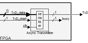
Async transmitter
It creates a signal "TxD" by serializing the data to transmit.
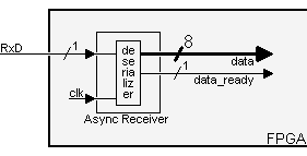
Async receiver
It takes a signal "RxD" from outside the FPGA and "de-serializes" it for easy use inside the FPGA.
This project has five parts
The project's code can be found here.
Serial interface 1 - How the RS-232 serial interface works
An RS-232 interface has the following characteristics:
- Uses a 9 pins connector "DB-9" (older PCs use 25 pins "DB-25").
- Allows bidirectional full-duplex communication (the PC can send and receive data at the same time).
- Can communicate at a maximum speed of roughly 10KBytes/s.
DB-9 connector
You probably already saw this connector on the back of your PC.

It has 9 pins, but the 3 important ones are:
- pin 2: RxD (receive data).
- pin 3: TxD (transmit data).
- pin 5: GND (ground).
Using just 3 wires, you can send and receive data.
Data is commonly sent by chunks of 8 bits (we call that a byte) and is "serialized": the LSB (data bit 0) is sent first, then bit 1, ... and the MSB (bit 7) last.
Asynchronous communication
This interface uses an asynchronous protocol. That means that no clock signal is transmitted along the data. The receiver has to have a way to "time" itself to the incoming data bits.
In the case of RS-232, that's done this way:
- Both side of the cable agree in advance on the communication parameters (speed, format...). That's done manually before communication starts.
- The transmitter sends "idle" (="1") when and as long as the line is idle.
- The transmitter sends "start" (="0") before each byte transmitted, so that the receiver can figure out that a byte is coming.
- The 8 bits of the byte data are sent.
- The transmitter sends "stop" (="1") after each byte.
Let's see how looks the byte 0x55 when transmitted:
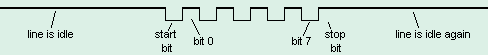
Byte 0x55 is 01010101 in binary.
But since it is transmitted LSB (bit-0) first, the line toggles like that: 1-0-1-0-1-0-1-0.
But since it is transmitted LSB (bit-0) first, the line toggles like that: 1-0-1-0-1-0-1-0.
Here's another example:
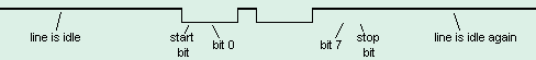
Here the data is 0xC4, can you see it?
The bits are harder to see. That illustrates how important it is for the receiver to know at which speed the data is sent.
The bits are harder to see. That illustrates how important it is for the receiver to know at which speed the data is sent.
How fast can we send data?
The speed is specified in baud, i.e. how many bits-per-seconds can be sent. For example, 1000 bauds would mean 1000 bits-per-seconds, or that each bit lasts one millisecond.
Common implementations of the RS-232 interface (like the one used in PCs) don't allow just any speed to be used. If you want to use 123456 bauds, you're out of luck. You have to settle to some "standard" speed. Common values are:
- 1200 bauds.
- 9600 bauds.
- 38400 bauds.
- 115200 bauds (usually the fastest you can go).
At 115200 bauds, each bit lasts (1/115200) = 8.7µs. If you transmit 8-bits data, that lasts 8 x 8.7µs = 69µs. But each byte requires an extra start and stop bit, so you actually need 10 x 8.7µs = 87µs. That translates to a maximum speed of 11.5KBytes per second.
At 115200 bauds, some PCs with buggy chips require a "long" stop bit (1.5 or 2 bits long...) which make the maximum speed drop to around 10.5KBytes per second.
Physical layer
The signals on the wires use a positive/negative voltage scheme.
- "1" is sent using -10V (or between -5V and -15V).
- "0" is sent using +10V (or between 5V and 15V).
So an idle line carries something like -10V.
Links
- An Introduction to RS232 Serial Communications
- Voltage Waveshapes, part of this huge Serial HOWTO
Serial interface 2 - Baud generator
Here we want to use the serial link at maximum speed, i.e. 115200 bauds (slower speeds would also be easy to generate). FPGAs usually run at MHz speeds, well above 115200Hz (RS-232 is pretty slow by today's standards). We need to find a way to generate (from the FPGA clock) a "tick" as close as possible to 115200 times a second.
Traditionally, RS-232 chips use a 1.8432MHz clock, because that makes generating the standard baud frequencies very easy... 1.8432MHz divided by 16 gives 115200Hz.
| // let's assume the FPGA clock signal runs at 1.8432MHz // we create a 4-bit counter reg [3:0] BaudDivCnt; always @(posedge clk) BaudDivCnt <= BaudDivCnt + 1; // count forever from 0 to 15 // and a tick signal that is asserted once every 16 clocks (so 115200 times a second) wire BaudTick = (BaudDivCnt==15); |
That was easy. But what do you do if instead of 1.8432MHz, you have a 2MHz clock? To generate 115200Hz from a 2MHz clock, we need to divide the clock by "17.361111111..." Not exactly a round number. The solution is to divide sometimes by 17, sometimes by 18, making sure the ratio stays "17.361111111". That's actually easy to do.
Look at the following "C" code:
| while(1) // repeat forever { acc += 115200; if(acc>=2000000) printf("*"); else printf(" "); acc %= 2000000; } |
That prints the "*" in the exact ratio, once every "17.361111111..." loops on average.
To obtain the same thing efficiently in an FPGA, we rely on the fact that the serial interface can tolerate a few % of error in the baud frequency generator.
It is desirable that the 2000000 be a power of two. Obviously 2000000 is not. So we change the ratio... Instead of "2000000/115200", let's use "1024/59" = 17.356. That's very close to our ideal ratio, and makes an efficient FPGA implementation: we use a 10-bit accumulator incremented by 59, with a tick marked everytime the accumulator overflows.
| // let's assume the FPGA clock signal runs at 2.0000MHz // we use a 10-bit accumulator plus an extra bit for the accumulator carry-out reg [10:0] acc; // 11 bits total! // add 59 to the accumulator at each clock always @(posedge clk) acc <= acc[9:0] + 59; // use 10 bits from the previous accumulator result, but save the full 11 bits result wire BaudTick = acc[10]; // so that the 11th bit is the accumulator carry-out |
Using our 2MHz clock, "BaudTick" is asserted 115234 times a second, a 0.03% error from the ideal 115200.
Parameterized FPGA baud generator
The previous design was using a 10 bits accumulator, but as the clock frequency increases, more bits are required.
Here's a design with a 25MHz clock and a 16 bits accumulator. The design is parameterized, so easy to customize.
| parameter ClkFrequency = 25000000; // 25MHz parameter Baud = 115200; parameter BaudGeneratorAccWidth = 16; parameter BaudGeneratorInc = (Baud<<BaudGeneratorAccWidth)/ClkFrequency; reg [BaudGeneratorAccWidth:0] BaudGeneratorAcc; always @(posedge clk) BaudGeneratorAcc <= BaudGeneratorAcc[BaudGeneratorAccWidth-1:0] + BaudGeneratorInc; wire BaudTick = BaudGeneratorAcc[BaudGeneratorAccWidth]; |
One last implementation issue: the "BaudGeneratorInc" calculation is wrong, due to the fact that Verilog uses 32 bits intermediate results, and the calculation exceeds that. Change the line as follow for a workaround.
| parameter BaudGeneratorInc = ((Baud<<(BaudGeneratorAccWidth-4))+(ClkFrequency>>5))/(ClkFrequency>>4); |
This line has also the added advantage to round the result instead of truncating.
Now that we have a precise enough Baud generator, we can go ahead with the RS-232 transmitter and receiver modules.
Serial interface 3 - RS-232 transmitter
We are building an "async transmitter" with fixed parameters: 8 data bits, 2 stop bits, no-parity.
It works like that:
- The transmitter takes an 8-bits data inside the FPGA and serializes it (starting when the "TxD_start" signal is asserted).
- The "busy" signal is asserted while a transmission occurs (the "TxD_start" signal is ignored during that time).
Serializing the data
To go through the start bit, the 8 data bits, and the stop bits, a state machine seems appropriate.
| reg [3:0] state; // the state machine starts when "TxD_start" is asserted, but advances when "BaudTick" is asserted (115200 times a second) always @(posedge clk) case(state) 4'b0000: if(TxD_start) state <= 4'b0100; 4'b0100: if(BaudTick) state <= 4'b1000; // start 4'b1000: if(BaudTick) state <= 4'b1001; // bit 0 4'b1001: if(BaudTick) state <= 4'b1010; // bit 1 4'b1010: if(BaudTick) state <= 4'b1011; // bit 2 4'b1011: if(BaudTick) state <= 4'b1100; // bit 3 4'b1100: if(BaudTick) state <= 4'b1101; // bit 4 4'b1101: if(BaudTick) state <= 4'b1110; // bit 5 4'b1110: if(BaudTick) state <= 4'b1111; // bit 6 4'b1111: if(BaudTick) state <= 4'b0001; // bit 7 4'b0001: if(BaudTick) state <= 4'b0010; // stop1 4'b0010: if(BaudTick) state <= 4'b0000; // stop2 default: if(BaudTick) state <= 4'b0000; endcase |
Now, we just need to generate the "TxD" output.
| reg muxbit; always @(state[2:0]) case(state[2:0]) 0: muxbit <= TxD_data[0]; 1: muxbit <= TxD_data[1]; 2: muxbit <= TxD_data[2]; 3: muxbit <= TxD_data[3]; 4: muxbit <= TxD_data[4]; 5: muxbit <= TxD_data[5]; 6: muxbit <= TxD_data[6]; 7: muxbit <= TxD_data[7]; endcase // combine start, data, and stop bits together assign TxD = (state<4) | (state[3] & muxbit); |
The complete code can be found here.
Serial interface 4 - RS-232 receiver
We are building an "async receiver":
Our implementation works like that:
- The module assembles data from the RxD line as it comes.
- As a byte is being received, it appears on the "data" bus. Once a complete byte has been received, "data_ready" is asserted for one clock.
Note that "data" is valid only when "data_ready" is asserted. The rest of the time, don't use it as new data may come that shuffles it.
Oversampling
An asynchronous receiver has to somehow get in-sync with the incoming signal (it normally doesn't have access to the clock used by the transmitter).
- To determine when a new data byte is coming, we look for the "start" bit by oversampling the signal at a multiple of the baud rate frequency.
- Once the "start" bit is detected, we sample the line at the known baud rate to acquire the data bits.
Receivers typically oversample the incoming signal at 16 times the baud rate. We use 8 times here... For 115200 bauds, that gives a sampling rate of 921600Hz.
Let's assume that we have a "Baud8Tick" signal available, asserted 921600 times a second.
The design
First, the incoming "RxD" signal has no relationship with our clock.
We use two D flip-flops to oversample it, and synchronize it to our clock domain.
We use two D flip-flops to oversample it, and synchronize it to our clock domain.
| reg [1:0] RxD_sync; always @(posedge clk) if(Baud8Tick) RxD_sync <= {RxD_sync[0], RxD}; |
We filter the data, so that short spikes on the RxD line aren't mistaken with start bits.
| reg [1:0] RxD_cnt; reg RxD_bit; always @(posedge clk) if(Baud8Tick) begin if(RxD_sync[1] && RxD_cnt!=2'b11) RxD_cnt <= RxD_cnt + 1; else if(~RxD_sync[1] && RxD_cnt!=2'b00) RxD_cnt <= RxD_cnt - 1; if(RxD_cnt==2'b00) RxD_bit <= 0; else if(RxD_cnt==2'b11) RxD_bit <= 1; end |
A state machine allows us to go through each bit received, once a "start" is detected.
| reg [3:0] state; always @(posedge clk) if(Baud8Tick) case(state) 4'b0000: if(~RxD_bit) state <= 4'b1000; // start bit found? 4'b1000: if(next_bit) state <= 4'b1001; // bit 0 4'b1001: if(next_bit) state <= 4'b1010; // bit 1 4'b1010: if(next_bit) state <= 4'b1011; // bit 2 4'b1011: if(next_bit) state <= 4'b1100; // bit 3 4'b1100: if(next_bit) state <= 4'b1101; // bit 4 4'b1101: if(next_bit) state <= 4'b1110; // bit 5 4'b1110: if(next_bit) state <= 4'b1111; // bit 6 4'b1111: if(next_bit) state <= 4'b0001; // bit 7 4'b0001: if(next_bit) state <= 4'b0000; // stop bit default: state <= 4'b0000; endcase |
Notice that we used a "next_bit" signal, to go from bit to bit.
| reg [2:0] bit_spacing; always @(posedge clk) if(state==0) bit_spacing <= 0; else if(Baud8Tick) bit_spacing <= bit_spacing + 1; wire next_bit = (bit_spacing==7); |
Finally a shift register collects the data bits as they come.
| reg [7:0] RxD_data; always @(posedge clk) if(Baud8Tick && next_bit && state[3]) RxD_data <= {RxD_bit, RxD_data[7:1]}; |
The complete code can be found here.
It has a few improvements; follow the comments in the code.
It has a few improvements; follow the comments in the code.
Links
- More details on Asynchronous Communication

沒有留言:
張貼留言