| Verilog Design: Harsha Perla Different ways to code Verilog: A Multiplexer example | |||||||||
There are different ways to design a circuit in Verilog. In this tutorial I have used seven different ways to implement a 4 to 1 MUX. After synthesizing, five of them gave same RTL level circuit in Xilinx Project navigator. Let us start with a block diagram of multiplexer.
| |||||||||
Example I
If select is 0, output q will be d[0]; if select is 1, q will be d[1]; if select is 2, q will be d[2] and if select is 3, q will be d[3]. This logic can be implemented using Verilog code as follows:
declaration 'input[1:0] select;' specifies select as port of 2 bits, with MSB select[1] and LSB select[0]. All the ports are declared as arrays because all the input signals must be declared as wires and left side of continuous statements should be wire. Actually, ports are wire by default and we need not declare it. But it is better to declare for our convenience.
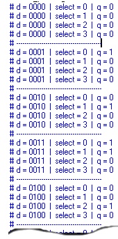
When select is 00, q will be assigned d[0], when select is 01, q will be assigned d[1] and so on. To test this, use following testbench. It generates a truth table with all possible values in the input and select.
 $monitor keeps displaying the values of its arguments whenever one of that changes. i.e., whenever values of d, select or q changes, it displays the value in the output window. Using a for loop, I have changed value of d from 0000 to 1111, and in each case change the value of select to all possible values. A part of output is as displayed the diagram in the right. $monitor keeps displaying the values of its arguments whenever one of that changes. i.e., whenever values of d, select or q changes, it displays the value in the output window. Using a for loop, I have changed value of d from 0000 to 1111, and in each case change the value of select to all possible values. A part of output is as displayed the diagram in the right.
Note that if we use for( d = 0; d <= 15; d = d + 1) instead of
for( i = 0; i <= 15; i = i + 1), for loop will go to infinite loop since d can never be greater that 15; so the condition d <= 15 will always be true.
Wave output of the above code taken from the ModelSim simulation is shown bellow.
You can use same test bench for all the multiplexer codes here. This output and wave diagrams are same for all the codes.
 Example II
This example is very similar to previous one, but instead of using continuous assignments, here alwaysstatement is used. left side of expressions inside an always block must be of register type. So, here q is declared s reg. When ever d or select changes, q should be changed to d[select]. So, d and select are added to the 'sensitivity list'. Even though we declared q is reg here, hardware register won't be used by synthesis tool to implement q. This is because always block here is combinational. Remember that if sensitivity list contains right hand side signals in the expressions and blocking statements are used, it will be combinational circuit when synthesising.
Use the same testbench as previous one for this code. Change mux1 my_mux by mux2 my_mux.
Example III
This example uses if statement of Verilog. Here also q is declared as reg and other signals as wire. This example also uses always block with the same sensitivity list. You can understand this code very easily.
Example IV Next example is also similar one. Here, case statement is used. case statement switches the execution of the code to corresponding block depending on the value of the parameter passed.
This example uses nested conditional statement. Meaning of the assign statement in the following code is "If select = 0, q = d[0], else if select is 1 q = d[1]. else if select is 2 q = d[2], else q = d[3]. We can use conditional statement inside always block also.
All the examples till now uses behavioral style of coding. Next example is data flow style of code.
Example VI
If we write an expression for 4 to 1 multiplexer, we can convert the expression in to code. Consider the expression bellow:
q = ( select[0].select[1].d[0] ) + ( select[0].select[1].d[1] ) + ( select[0].select[1].d[2] ) + ( select[0].select[1].d[3] )
You can write a truth table to verify the equation. Now we can write a code using Verilog for this equation as follows. We can also use assign statement instead of writing always block.
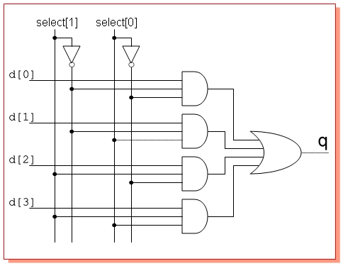
This example is gate level implementation of the multiplexer. All basic gates are declared in Verilog. We can instantiate them to get a gate level circuit. Let us draw the diagram of multiplexer first.

Now, convert the circuit in to code. instantiate 2 NOT gates, four AND gates and one OR gate as in the diagram. All the outputs from the gates should be wire. Hence code contains all the signals as wires.
More tutorials on Verilog is to be added soon. | |||||||||
2012年10月11日 星期四
Different ways to code Verilog: A Multiplexer example
訂閱:
張貼留言 (Atom)
8-QAM Signal 4 Phases 2 Amplitudes + 8PSK
8-QAM Signal 4 Phases 2 Amplitudes + 8PSK import tkinter as tk from tkinter import messagebox import math import cmath # --- 8-QAM 參數設定 ---...

-
python pip 不是内部或外部命令 -- 解決方法 要安裝 Pyqt5 1. 首先,開啟命令提示字元。 2. 輸入 pip3 install pyqt5 好像不能執行 ! ! 錯誤顯示 : ‘ pip3 ’ 不是內部或外部命令、可執行的程式或批...
-
課程講義 下載 11/20 1) PPT 下載 + 程式下載 http://www.mediafire.com/file/cru4py7e8pptfda/106%E5%8B%A4%E7%9B%8A2-1.rar 11/27 2) PPT 下載...
-
• 認 識 PreFix、InFix、PostFix PreFix(前序式):* + 1 2 + 3 4 InFix(中序式): (1+2)*(3+4) PostFix(後序式):1 2 + 3 4 + * 後 序式的運算 例如: 運算時由 後序式的...

沒有留言:
張貼留言