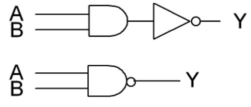
Logic Circuit of the NAND gate
Gate Level modeling
module NAND_2_gate_level(output Y, input A, B);
    wire Yd;
    and(Yd, A, B);
    not(Y, Yd);
endmodule
Data flow modeling
module NAND_2_data_flow (output Y, input A, B);
    assign Y = ~(A & B);
endmodule
Behavioral Modeling
NAND gate’s truth table
| A | B | Y(A nand B) |
| 0 | 0 | 1 |
| 0 | 1 | 1 |
| 1 | 0 | 1 |
| 1 | 1 | 0 |
Equation from the truth table
Y = (A.B)’ or say Y = (A & B)’.
module NAND_2_behavioral (output reg Y, input A, B);
always @ (A or B) begin
    if (A == 1'b1 & B == 1'b1) begin
        Y = 1'b0;
    end
    else
        Y = 1'b1;
end
endmodule
RTL schematic of the NAND gate
Have a look at the schematic.

Testbench of the NAND gate using Verilog
`include "NAND_2_behavioral.v"
`timescale 100ns/1ns
module NAND_2_behavioral_tb;
reg A, B;
wire Y;
NAND_2_behavioral Indtance0 (Y, A, B);
initial begin
    A = 0; B = 0;
 #1 A = 0; B = 1;
 #1 A = 1; B = 0;
 #1 A = 1; B = 1;
end
initial begin
    $monitor ("%t | A = %d| B = %d| Y = %d", $time, A, B, Y);
    $dumpfile("dump.vcd");
    $dumpvars();
end
endmodule

沒有留言:
張貼留言