參考來源 https://www.geeksforgeeks.org/carry-look-ahead-adder/
參考來源 https://www.nandland.com/vhdl/modules/carry-lookahead-adder-vhdl.html


module carry_look_ahead_adder
(
input [3:0] i_add1,
input [3:0] i_add2,
output [4:0] o_result
);
wire [4:0] w_C;
wire [3:0] w_G, w_P, w_SUM;
full_adder full_adder_bit_0
(
.i_bit1(i_add1[0]),
.i_bit2(i_add2[0]),
.i_carry(w_C[0]),
.o_sum(w_SUM[0]),
.o_carry()
);
full_adder full_adder_bit_1
(
.i_bit1(i_add1[1]),
.i_bit2(i_add2[1]),
.i_carry(w_C[1]),
.o_sum(w_SUM[1]),
.o_carry()
);
full_adder full_adder_bit_2
(
.i_bit1(i_add1[2]),
.i_bit2(i_add2[2]),
.i_carry(w_C[2]),
.o_sum(w_SUM[2]),
.o_carry()
);
full_adder full_adder_bit_3
(
.i_bit1(i_add1[3]),
.i_bit2(i_add2[3]),
.i_carry(w_C[3]),
.o_sum(w_SUM[3]),
.o_carry()
);
// Create the Generate (G) Terms: Gi=Ai*Bi
assign w_G[0] = i_add1[0] & i_add2[0];
assign w_G[1] = i_add1[1] & i_add2[1];
assign w_G[2] = i_add1[2] & i_add2[2];
assign w_G[3] = i_add1[3] & i_add2[3];
// Create the Propagate Terms: Pi=Ai+Bi
assign w_P[0] = i_add1[0] | i_add2[0];
assign w_P[1] = i_add1[1] | i_add2[1];
assign w_P[2] = i_add1[2] | i_add2[2];
assign w_P[3] = i_add1[3] | i_add2[3];
// Create the Carry Terms:
assign w_C[0] = 1'b0; // no carry input
assign w_C[1] = w_G[0] | (w_P[0] & w_C[0]);
assign w_C[2] = w_G[1] | (w_P[1] & w_C[1]);
assign w_C[3] = w_G[2] | (w_P[2] & w_C[2]);
assign w_C[4] = w_G[3] | (w_P[3] & w_C[3]);
assign o_result = {w_C[4], w_SUM}; // Verilog Concatenation
endmodule // carry_lookahead_adder_4_bit
module full_adder
(
i_bit1,
i_bit2,
i_carry,
o_sum,
o_carry
);
input i_bit1;
input i_bit2;
input i_carry;
output o_sum;
output o_carry;
wire w_WIRE_1;
wire w_WIRE_2;
wire w_WIRE_3;
assign w_WIRE_1 = i_bit1 ^ i_bit2;
assign w_WIRE_2 = w_WIRE_1 & i_carry;
assign w_WIRE_3 = i_bit1 & i_bit2;
assign o_sum = w_WIRE_1 ^ i_carry;
assign o_carry = w_WIRE_2 | w_WIRE_3;
// FYI: Code above using wires will produce the same results as:
// assign o_sum = i_bit1 ^ i_bit2 ^ i_carry;
// assign o_carry = (i_bit1 ^ i_bit2) & i_carry) | (i_bit1 & i_bit2);
// Wires are just used to be explicit.
endmodule // full_adder
// 時間單位 100ns, 時間精確度100 ps
`timescale 100ns/100ps
module Test_bench;
parameter WIDTH = 4;
reg [WIDTH-1:0] r_ADD_1 = 0;
reg [WIDTH-1:0] r_ADD_2 = 0;
wire [WIDTH:0] w_RESULT;
//module carry_look_ahead_adder
// input [3:0] i_add1,
// input [3:0] i_add2,
// output [4:0] o_result
carry_look_ahead_adder UUT(.i_add1(r_ADD_1),.i_add2(r_ADD_2),.o_result(w_RESULT));
initial
begin
#30;
r_ADD_1 = 4'b1000;
r_ADD_2 = 4'b1001;
#30;
r_ADD_1 = 4'b1010;
r_ADD_2 = 4'b1010;
#30;
r_ADD_1 = 4'b1101;
r_ADD_2 = 4'b1110;
#30;
r_ADD_1 = 4'b0101;
r_ADD_2 = 4'b1010;
#30;
r_ADD_1 = 4'b0101;
r_ADD_2 = 4'b0110;
#30;
r_ADD_1 = 4'b1111;
r_ADD_2 = 4'b1111;
#30;
end
initial begin
#220 $stop;
end
endmodule // carry_lookahead_adder_tb
Carry Look-Ahead Adder
Motivation behind Carry Look-Ahead Adder :
In ripple carry adders, for each adder block, the two bits that are to be added are available instantly. However, each adder block waits for the carry to arrive from its previous block. So, it is not possible to generate the sum and carry of any block until the input carry is known. The block waits for the
  block to produce its carry. So there will be a considerable time delay which is carry propagation delay.
In ripple carry adders, for each adder block, the two bits that are to be added are available instantly. However, each adder block waits for the carry to arrive from its previous block. So, it is not possible to generate the sum and carry of any block until the input carry is known. The
block waits for the block to produce its carry. So there will be a considerable time delay which is carry propagation delay.
Consider the above 4-bit ripple carry adder. The sum  is produced by the corresponding full adder as soon as the input signals are applied to it. But the carry input
  is not available on its final steady state value until carry
  is available at its steady state value. Similarly depends on
  and on
  . Therefore, though the carry must propagate to all the stages in order that output
  and carry settle their final steady-state value.
is produced by the corresponding full adder as soon as the input signals are applied to it. But the carry input is not available on its final steady state value until carry is available at its steady state value. Similarly depends on and on . Therefore, though the carry must propagate to all the stages in order that output and carry settle their final steady-state value.
The propagation time is equal to the propagation delay of each adder block, multiplied by the number of adder blocks in the circuit. For example, if each full adder stage has a propagation delay of 20 nanoseconds, then will reach its final correct value after 60 (20 × 3) nanoseconds. The situation gets worse, if we extend the number of stages for adding more number of bits.
will reach its final correct value after 60 (20 × 3) nanoseconds. The situation gets worse, if we extend the number of stages for adding more number of bits.
Carry Look-ahead Adder :
A carry look-ahead adder reduces the propagation delay by introducing more complex hardware. In this design, the ripple carry design is suitably transformed such that the carry logic over fixed groups of bits of the adder is reduced to two-level logic. Let us discuss the design in detail.
A carry look-ahead adder reduces the propagation delay by introducing more complex hardware. In this design, the ripple carry design is suitably transformed such that the carry logic over fixed groups of bits of the adder is reduced to two-level logic. Let us discuss the design in detail.
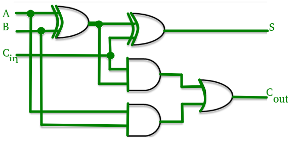

Consider the full adder circuit shown above with corresponding truth table. We define two variables as ‘carry generate’  and ‘carry propagate’
  then,
then,
and ‘carry propagate’ then,
The sum output and carry output can be expressed in terms of carry generate and carry propagate as
and carry propagate aswhere
produces the carry when both  ,
,  are 1 regardless of the input carry. is associated with the propagation of carry from
  to
to  .
.
The carry output Boolean function of each stage in a 4 stage carry look-ahead adder can be expressed as

From the above Boolean equations we can observe that does not have to wait for and to propagate but actually is propagated at the same time as and . Since the Boolean expression for each carry output is the sum of products so these can be implemented with one level of AND gates followed by an OR gate.
does not have to wait for and to propagate but actually is propagated at the same time as and . Since the Boolean expression for each carry output is the sum of products so these can be implemented with one level of AND gates followed by an OR gate.
The implementation of three Boolean functions for each carry output (, and ) for a carry look-ahead carry generator shown in below figure.
, and ) for a carry look-ahead carry generator shown in below figure.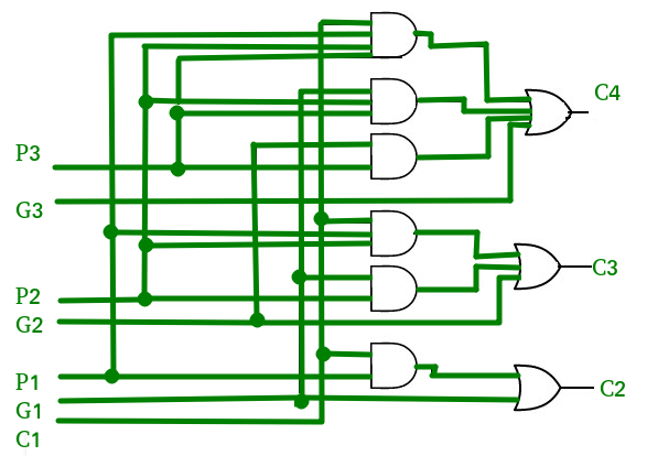
Time Complexity Analysis :
We could think of a carry look-ahead adder as made up of two “parts”
We could think of a carry look-ahead adder as made up of two “parts”
- The part that computes the carry for each bit.
- The part that adds the input bits and the carry for each bit position.
The  complexity arises from the part that generates the carry, not the circuit that adds the bits.
Now, for the generation of the carry bit, we need to perform a AND between (n+1) inputs. The complexity of the adder comes down to how we perform this AND operation. If we have AND gates, each with a fan-in (number of inputs accepted) of k, then we can find the AND of all the bits in
  time. This is represented in asymptotic notation as
  .
.
complexity arises from the part that generates the carry, not the circuit that adds the bits.Now, for the generation of the
carry bit, we need to perform a AND between (n+1) inputs. The complexity of the adder comes down to how we perform this AND operation. If we have AND gates, each with a fan-in (number of inputs accepted) of k, then we can find the AND of all the bits in time. This is represented in asymptotic notation as .
Advantages and Disadvantages of Carry Look-Ahead Adder :
Advantages –
Advantages –
- The propagation delay is reduced.
- It provides the fastest addition logic.
Disadvantages –
- The Carry Look-ahead adder circuit gets complicated as the number of variables increase.隨著變量數量的增加,進位超前加法器電路變得複雜。
- The circuit is costlier as it involves more number of hardware.該電路較昂貴,因為它涉及更多的硬件。


沒有留言:
張貼留言