Hierarchical Designing: A Hierarchical methodology is used to design simple components to construct more complex component. The key idea is to divide and conquer i.e. to divide the big complex circuit into smaller modules and further dividing these modules to even smaller modules like gates etc.
There are two design approaches when writing code in hierarchical style
- Top-Down Methodology
- Bottom-Up Methodology
Top-Down Methodology: In Top-Down we first identify or define the big circuit or big block and then identify a small block used to make this big block. We further divide the small block to leaf cells which cannot be further divided. e.g. you want to construct full adder, so you immediately identify two small blocks i.e. half adder.
Bottom-Up Methodology: In this approach, we first identify small blocks that are available to us and use them to construct a big block. E.g., you have two half adders available, and you can construct a full adder using these two half adders.
Typically designers use these two approaches side-by-side to construct complex circuits. Design architects define the specifications of the top-level block. Logic designers decide how the design should be structured by breaking up the functionality into blocks and sub-blocks. At the same time, circuit designers are designing optimized circuits for leaf-level cells. They build higher-level cells by using these leaf cells.
Instance: Before proceeding towards examples, we would like to clarify the concept of “instance”. An instance is a copy of a module created when a big component calls a smaller component. An instance must have a unique name. The following examples will help you clarify the concept of instantiation and hierarchical designing.
Example-1: Design and simulate Half-Adder using gate-level modelling.
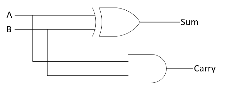
Truth Table: Given below is the truth table for half adder:

From the above table of Half adder we can construct its boolean expression given below:
Hence gate-level diagram constructed as:
Verilog Code:
TestBench Code:
The above code is written for half adder you may see no hierarchical style coding in it as half adder cannot be further divided but we can construct full adder by using two half adder which is shown below as well. But first lets see its simulated waveform:
Simulated Waveform of Half Adder


沒有留言:
張貼留言