Working with the Comparator Circuit
源自於 http://www.ermicro.com/blog/?p=1578
Sometimes in the embedded system world we need to process the analog world and sending the signal to the microcontroller when the analog signal exceed some predetermine limit we’ve set. Some example of this situation is to send the interrupt signal to the microcontroller operation when the temperature is already exceeds certain limit or the light intensity exceeds certain bright level. This is when the comparator circuit becomes handy as it’s designed specially for this purpose.
Today the modern comparator is easily found in the form of integrated circuit such as the popular National Semiconductor LM339 quad (four) comparator 14 pins dual in line (DIL) package bellow:

When you look closely to the comparator symbol, some of you will recognize it as the Op-Amp (Operational Amplifier) symbol, so what make this comparator differ from its big brother; Op-Amps is designed to accept the analog signal and outputting the analog signal while the comparator only outputting the digital signal; although the ordinary Op-Amp could be used as the comparator such as the popular National Semiconductor LM324 quad Op-Amps, but the real comparator is designed to have a faster switching time comparing to the multipurpose Op-Amps. Therefore you could say that the comparator is the modified version of the Op-Amps which specially designed to give the digital output.
1. Basic Comparator Circuit
The comparator circuit work by simply taking two analog inputs, comparing them and produce the logical output high “1” or low “0“.
By applying the analog signal to the comparator + input called “non-inverting” and - input called “inverting“, the comparator circuit will compared this two analog signal, if the analog input on + input is greater than the analog input on - input (inverting) then the output will swing to the logical “1” and this will make the open collector transistor Q8 on the LM339 equivalent circuit above to turn ON. When the analog input on + input (non inverting) is less than the analog input on - input(inverting) then the comparator output will swing to the logical “0” (the Q8 transistor turn OFF). Furthermore on this tutorial, I will use the term non-inverting and inverting instead of + inputand - input on the comparator analog input.
As you’ve seen from the LM339 equivalent circuit picture above, the LM339 use an open collector transistor Q8 for its output, therefore we have to use what is called “pull-up” resistor connected to the Q8 collector lead with the Vcc in order to make this Q8 transistor work. The maximum current that could flow on this Q8 transistor (output sink current) according to the LM339 datasheet is about 18 mA.
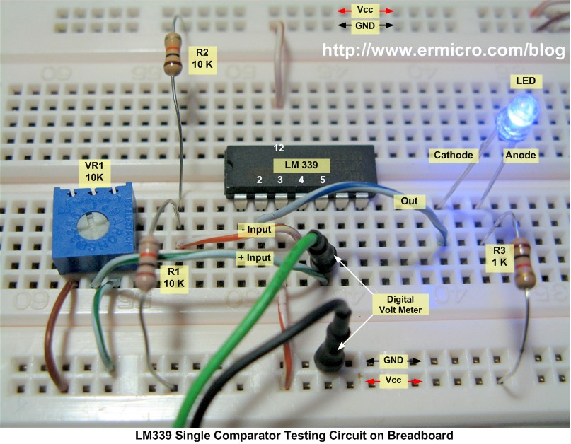
The testing circuit simply connects the comparator inverting input to the voltage divider R1 and R2, with 5 Volt voltage supply the V- could be calculated as follow:
V- = (R2 / (R1 + R2)) x Vcc
V- = (10 / 20) x 5 volt = 2.5 volt
V- = (10 / 20) x 5 volt = 2.5 volt
For more information about the voltage divider circuit please refer to my previous posted blog Basic Resistor Circuit.
The comparator non-inverting input is connected to the 10 K trimport which is also forming the voltage divider circuit where we could adjust the V+ voltage start from 5 volt down to 0 volt. First when the V+ is equal to Vcc (5 volt) the comparator output will swing to the logical high (Vout = Vcc) because the V+ is greater than V- (2.5 volt). This will switch the Q8 transistor OFF and the LED will turn OFF. When the voltage V+ drop bellow 2.5 volt, the comparator output will swing to the logical low (Vout = GND) and this will switch the Q8 transistor ON and the LED will turn ON.
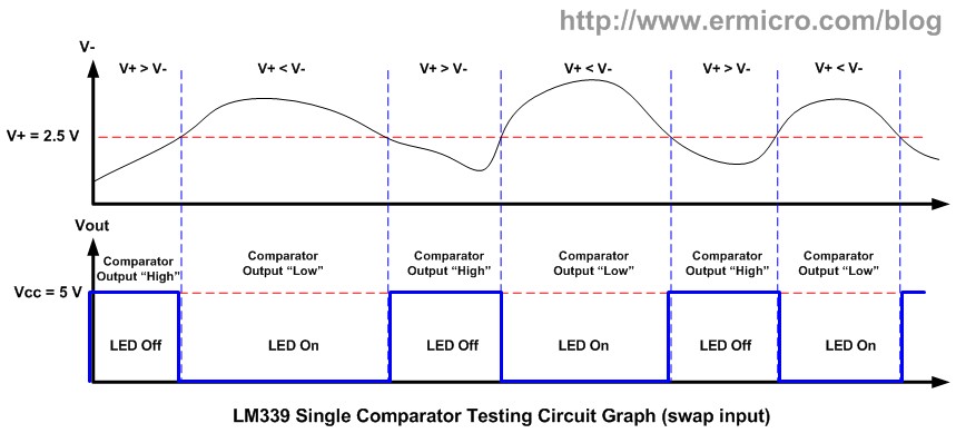
By swapping the analog input; the R1 and R2 voltage divider connected to the non-inverting input (V+) and the trimport connected to the inverting input (V-) we will get the opposite output result.
Again using the voltage divider principal the voltage on the non-inverting input (V+) is about 2.5 volt, therefore if we start the inverting input voltage (V-) at 5 volt; the V+ is lower than the V-, this will make the comparator output will swing to the logical low (the Q8 transistor ON) and the LED will turn ON. When we adjust the V- down bellow the 2.5 volt (V+) than the comparator output will swing to the logical high (the Q8 transistor OFF) because the V+ now is greater than V- and the LED will turn OFF. You could see all of this experiment on the video at the end of this tutorial.
As you’ve seen from the experiment above, the comparator is usually used to compare one variable analog signal with predetermined analog signal or we could call it as the reference voltage. Therefore by placing the reference voltage to the inverting or non-inverting input we could manage the comparator output accordance to our need. This comparator circuit is also known as the zero crossing detector circuit.
The following schema show you how we utilized the zero crossing detector circuit in the infra-red reflective detector usually found in many robotics projects.
When the infra-red LED beam reflected back to the photo transistor, the photo transistor will turn ON; this will make the reference voltage (V+) become greater than the input voltage (V-). This condition will make the comparator give a logical high to the microcontroller I/O port. When the infra-red LED beam is blocked, the photo transistor will turn OFF; this will make the input voltage (V-) become greater than the reference voltage (V+) and the comparator will give a logical low to the microcontroller I/O port.
Hmm, by applying the circuit schema above to all the comparators in the LM339 package (four comparators), we could make a very sensitive infrared reflector sensors for sensing the black/white line used in many line follower or line maze solver robot.
2. Comparator with the Positive Feedback
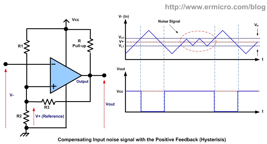
One of the drawbacks with the zero crossing detector on the circuit above is; it’s very sensitive to the noise signal (small interference signal) on its input as shown on this following picture:
Because the comparator basically is an uncompensated high gain operational amplifier, therefore this could make the comparator to start oscillate or continuously giving high and low output. To compensate this behavior we could apply a small amount of voltage feedback to the non-inverting input as shown on this following schema:
To analyze this circuit first we assume the output voltage is high; in order to meet this condition theV- (inverting input) voltage should be lower than the V+ (non-inverting input) voltage. When the V-voltage increases toward the V+ voltage, this will drive the Vout toward ground which will also shift the V+ voltage through the R3 resistor. Because the V+ is the non-inverting input to the comparator; this feedback will help to drive down the Vout to ground even faster. The opposite condition also occur when the V- voltage decrease, because of the R3 resistor feedback on the V+input; this feedback will shift the V+ voltage input will ensure a faster switching result to logical high (Vcc) on the Vout.
The V+ voltage upper threshold (VUT) to make the Vout voltage to swing to ground could be calculated as this following formula.
VUT = (R2 / (R2 + R1||R3)) x Vout
We assume the Vout equal to Vcc when the output is high then we could have this following formula:
VUT = (R2 / (R2 + R1||R3)) x Vcc
and
R1||R3 = (R1 x R3) / (R1 + R3).
Substituting the R1||R3 (R1 parallel R3) inside this equation we will get this following formula:
VUT = (Vcc x R2 x (R1 + R3)) / (R1 x R2 + R1 x R3 + R2 x R3).
The V+ voltage lower threshold (VLT) to make the Vout voltage to swing to high (Vcc) could be calculated as this following formula.
VLT = (R2||R3 / (R2||R3 + R1)) x Vcc
and
and
R2||R3 = (R2 x R3) / (R2 + R3).
Again by substituting the R2||R3 (R2 parallel R3) inside this equation we will get this following formula:
VLT = (Vcc x R2 x R3) / (R1 x R2 + R1 x R3 + R2 x R3).
The different between the upper and lower threshold voltage is called the hysteresis voltage:
VH = VUT – VLT
Therefore by applying the upper and lower threshold formula, we could get the hysteresis voltage as follow:
VH = (Vcc x R1 x R2) / (R1 x R2 + R1 x R3 + R2 x R3).
To insure that Vout will swing between Vcc and ground we have to choose:
R3 > R pull-up and R pull-up < R load
Therefore by assigning the R pull-up = 10K, R1 = R2 = R3 = 100K and using the 5 volt supply we could calculate the upper and lower threshold voltage as follow:
VUT = 2/3 Vcc and VLT = 1/3 Vcc
The different between the upper and lower threshold is called the hysteresis voltage:
VH = 1/3 Vcc
The common way to represent the hysteresis graph instead of using two graphs as shown on the above picture is by assigning the Vout on the Y axis and V- (in) on the X axis, now we could get this following picture:
Therefore by shifting the V+ voltage with the R3 feedback resistor we could compensate the comparator output to become more immune to the noise signal. This hysteresis comparator circuit also could be used as a Schmitt Trigger with the adjustable threshold point by just changing the value of R1, R2 and R3 resistors respectively.
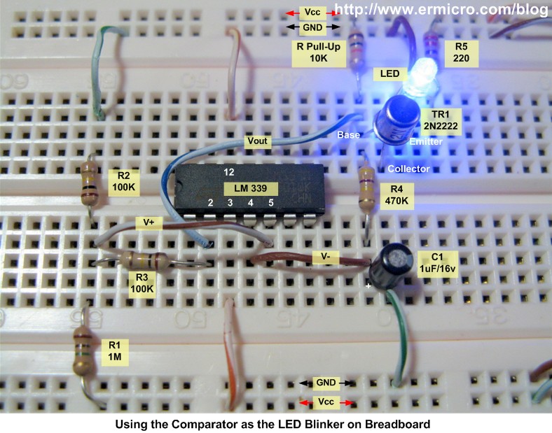
One of the interesting usages of this hysteresis behavior is to use the comparator as the pulse generator or oscillator; where you could easily make a simple LED blinker as shown on this following circuit bellow:
Again to analyze this circuit first we assume the Vout is high, this will turn on the TR1 transistor and the LED will be ON. In order to meet this condition the V- should be less than V+ (V- almost zero) or we could say that the C1 is now being charged through the R4 resistor. Now the V- will slowly increase and because of the voltage shift provided by the R3 feedback resistor on the V+ input; this will make the Vout rapidly swing to the logical low (LED OFF) and this time the C1 will discharge its energy through the R4 resistor and the V- will decrease; when it reach bellow the V+ then the process will repeat again. You could easily change the LED blink rate by changing the R4 and C1 value respectively.
The output frequency could be calculated using this following formula (taken from AN-74: National Semiconductor Application Note 74):

Where R4 is the resistance in Ohm, C1 is the capacitance in Farad and freq. is the pulse frequency in Hertz. Therefore using this formula, we could calculate the frequency of the LED blinker circuit above as follow:
1 / Freq. = 2 (0.694) x 470000 x 0.0000001 = 0.65236
Frequency = 1 / 0.65236 = 1.53 Hertz
Frequency = 1 / 0.65236 = 1.53 Hertz
By using different R4 and C1 values on each comparator in the LM339 package (four comparators) you could assembly four independent LED blinker with each of them have a different blink rate. By hooking up to 4 LEDs on each 2N2222 transistor you could get a very nice random LED blink effect similar to the main computer panel shown on many sci-fi movies.
3. The Limit Window Comparator
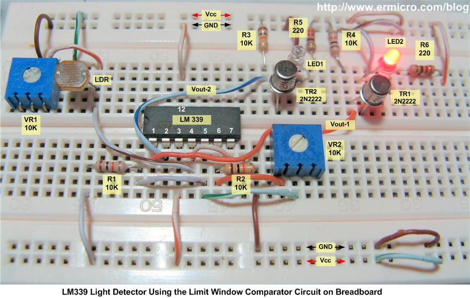
Using a single comparator we could only have one voltage reference value, if we want to have two voltage reference values; where we could set the upper and lower voltage level limit value to determine the output; we could used what is called the limit window comparator circuit or also known as dual edge limit detector circuit. On our next experiment we will build the light sensor circuit with the LDR (light dependent resistor) as the sensor and using the limit window comparator circuit. This circuit will light up the LED according to the light intensity detected by LDR. The complete example circuit is shown on this following schema:
To analyze the circuit above; first we assume that the VR2 is equal to 10K; Again the R1, VR2 and R2 will form the voltage divider circuit to both V1 and V2:
V1 = ((R2 + VR2) / (R1 + VR2 + R2)) x Vcc = 2/3 Vcc
V2 = (R2 / (R1 + VR2 + R2)) x Vcc = 1/3 Vcc
V2 = (R2 / (R1 + VR2 + R2)) x Vcc = 1/3 Vcc
The LDR and the VR1 are also forming the voltage divider circuit on the Vin:
Vin = (VR1 / (VR1 + LDR) x Vcc
Therefore if Vin is greater than V1 and V2 (Vin > 2/3 Vcc) then the comparator CMP1 output will swing to the logical low and make the TR2 to turn OFF (LED2 OFF), while the comparator CMP2 output will swing to the logical high, this will power the TR1 base make the TR1 to turn ON (LED2 ON).
When the Vin is less then V1 but greater than V2 (1/3 Vcc < Vin < 2/3 Vcc) then the comparator CMP1 output will swing to logical high and make the TR2 to turn ON (LED2 ON). The comparator CMP2 output also will swing to the logical high, this will provide the necessary voltage input on the TR1 base to make it ON (LED1 ON).
The last when the Vin voltage goes bellow the V1 and V2 (Vin < 1/3 Vcc) then the comparator CMP1 output will swing to logical high and make the TR2 to turn ON (LED2 ON), while the comparator CMP2 output will swing to the logical low and make the TR1 to turn OFF (LED1 OFF).
Therefore by adjusting the VR1 and VR2 you could easily adjust the Vin and set the upper and lower voltage reference level limit as necessary.
By connecting both comparator open collector output (wired-OR) we could get the desired response, where the output only swing to the logical high (“1“) when Vin voltage is within the Lower and Upper limit voltage.
The limit window comparator mostly used to detect two conditions such as for the temperature sensor, when the temperature exceed the upper limit or way down below the lower limit; the limit window comparator output will send the warning or control signal to the microcontroller I/O port
4. Comparator inside the Microcontroller
On this last comparator tutorial we will take a look at the comparator circuit inside the microcontroller. Most of today’s modern microcontroller has already equipped with this feature. Usually it being used as the zero crossing detector circuit, where it takes two analog inputs and compares them; then produce the interrupt according to the voltage input level on both input.
Now let’s take a look at the Atmel AVR ATTiny25 microcontroller; it’s one of the smallest and yet powerful 8-bit 8-pins AVR family microcontroller which has a build in one powerful analog comparator circuit inside.
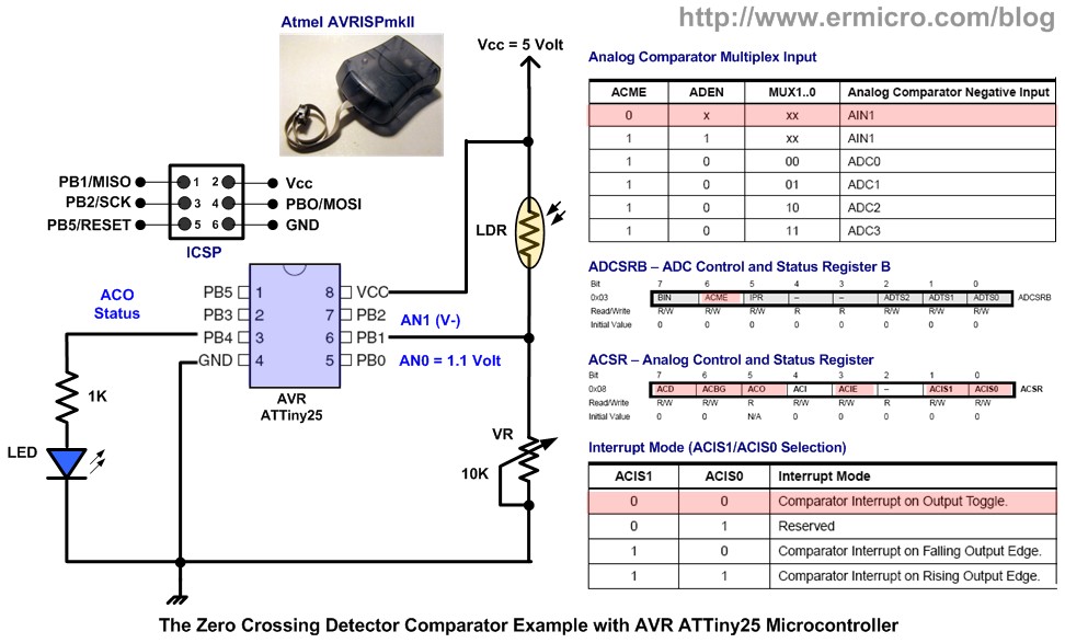
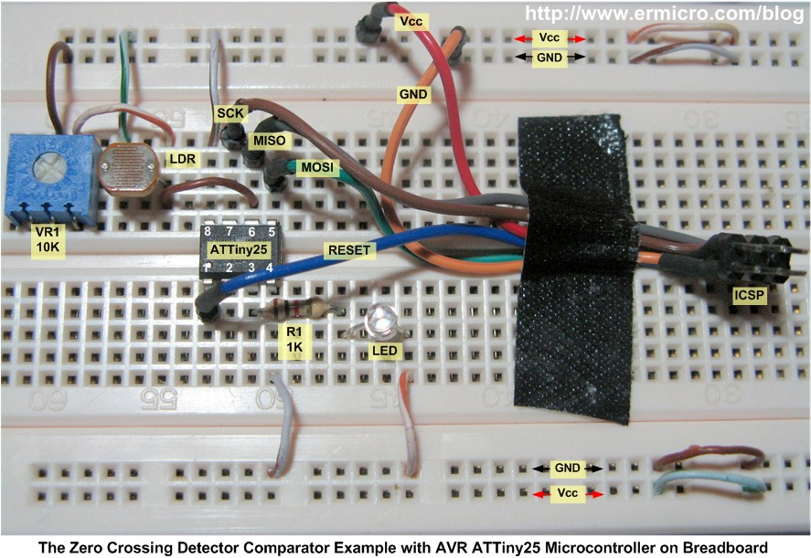
The AIN0 (PB0) could be used as the comparator’s non-inverting input and the AIN1 (PB1) could be used as the comparator inverting input. We also could choose to use the AVR ATTiny25 microcontroller internal reference voltage 1.1 volt connected to the non-inverting input. To understand how this analog comparator works, I use a simple circuit to demonstrate how we could use the microcontroller analog comparator as the zero crossing detectors. This time I will take advantage of the internal reference voltage on the non-inverting input and connect the comparator inverting input to the LDR and trimport. This following schema shows you the example of light detector using the ATTiny25 microcontroller analog comparator feature.
The following is the AVR microcontroller assembler code that demonstrates this capability:
;***************************************************************************
; File Name    : comparator.asm
; Version      : 1.0
; Description. : Zero Crossing Detector Examples
; Author       : RWB
; Target       : AVR ATTiny25
; Compiler     : AVR macro assembler 2.1.41 (build 1792)
; IDE          : Atmel AVR Studio 4.17
; Programmer   : Atmel AVRISPmkII
; Last Updated : 01 March 2010
;***************************************************************************
.include "tn25def.inc"
; Use AVR ATTiny25 Default Frequency Clock
.equ F_CPU = 8000000
.cseg
; Start on the flash ram's address 0
.org 0
        rjmp  main             ; Jump to the Main Program
.org    ACIaddr                ; 0x0007 - Analog Comparator Interrupt Vector
        rjmp  a_comp           ; Jump to Analog Comparator Interrupt Handler
; Analog Comparator Interrupt Routine Handler
a_comp: in    R0,SREG          ; Save the SREG Status
        sbic  ACSR,ACO         ; if (AC0 == 0), V- > 1.1V, Turn Off LED
        rjmp  led_on           ; else, V- < 1.1 V, Turn On LED
        cbi   PORTB,PB4        ; Turn Off LED on PB4
        rjmp  ex_int           ; Goto Exit Interrupt
led_on: sbi   PORTB,PB4        ; Turn On LED on PB4
ex_int: out   SREG,R0          ; Restore the SREG Status
        reti                   ; Return from Interrupt Handler
; Start the Main Program
main:   ldi   R24,RAMEND       ; Initial Stack Pointer
        out   SPL,R24          ; SP = RAMEND
; Initial the I/O Used
        ldi   R16,0b00010000   ; Set PB4=Output, PB0,PB1,PB2,PB3,PB5 and PB6 as Input
        out   DDRB,R16         ; DDRB=0x10
; Initial the Analog Comparator
        cbi   ADCSRB,ACME      ; Disable Multiplex Inverting input, just use AN1 (PB1)
        cbi   ACSR,ACD         ; Enable Analog Comparator
        sbi   ACSR,ACBG        ; Use 1.1V (Band Gap) Internal Reference on AN0-Non Inverting Input
        cbi   ACSR,ACIS1       ; Use Interrupt Output Toggle
        cbi   ACSR,ACIS0
        ldi   R16,0b00000011   ; Disable Digital Input on AN0 (PB0) and AN1 (PB1)
        out   DIDR0,R16
        sbi   ACSR,ACIE        ; Enable Analog Comparator Interrupt
        sei                    ; Enable Global Interrupt
loop: rjmp loop ; Loop Forever and Let the Interrupt do the work
.exit
; EOF: comparator.asm
The analog comparator inside the Atmel AVR ATTiny25 microcontroller is capable to use multiplex inverting analog input from ADC0, ADC1, ADC2 and ADC3, but on this tutorial I will use the AN1(PB1) as the inverting input which connected to the LDR and 10 K trimport voltage divider circuit. By clearing the ACME (Analog Comparator Multiplex Enable) bit on the ADCSRB register, we simply disable this feature.
The non-inverting input is designed to use the 1.1 volt internal reference voltage by enabling the analog comparator band gap (ACBG) bit on the ACSR register. By enabling the analog comparator interrupt (ACIE) bit on the ACSR register, we could instruct the AVR ATTiny25 microcontroller to generate interrupt on every output toggle by clearing the ACIS1 and ACIS0 bits on the ACSRregister. Therefore by examining the analog comparator output (ACO) bit on the ACSR register we could easily determine whether the V- inverting voltage (AN1) is less or greater than the V+ (AN0) inverting voltage and use this information to toggle the PB4 output port to make the LED ON and OFF. You could read more about programming the AVR assembler code on my previous posted blogBeginners AVR Assembler Language Programming 1
Using the powerful Atmel AVR Studio v4.17 integrated development environment you could easily compile and debug this AVR assembler code, and then down load the hex code into the ATTiny25 microcontroller flash ram using the AVR microcontroller programmer; on this tutorial I used Atmel AVRISPmkII programmer.
Now you could enjoy this following video which showing all the experiments we’ve already done on this tutorial
The Final Thought
The comparator or op-amps in general is one of the breakthroughs in the integrated circuit development as this tiny smart circuit has tremendous applications in electronics industries. Therefore understanding of how the comparator work will help you take the advantage of this amazing circuit in your next electronics or embedded system project.












沒有留言:
張貼留言