Flip-flops
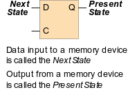
All useful memory devices have at least two inputs—one for the data signal to be memorized, and a timing control signal to define exactly when the data signal should be memorized. As shown Fig. 1, the current output of a memory device is called the “present state”, and the input is called the “next state” because it will define the memory at the next assertion of the timing control input. In a D-latch, the present state and next state are the same as long as the timing control input is asserted. A D flip-flop modifies the function of a D-latch in a fundamental and important way: the next state (or D input) can only be written into the memory on the edge (or transition) of the timing signal.

 A D flip-flop (DFF) is one of the most fundamental memory devices. A DFF typically has three inputs: a data input that defines the next state, a timing control input that tells the flip-flop exactly when to “memorize” the data input, and a reset input that can cause the memory to be reset to '0', regardless of the other two inputs. The 'D' in DFF arises from the name of the data input; thus, the flip-flop may also be called a data flip-flop. The timing control input, called “clock”, is used to coordinate when new data can be written into the memory element, and conversely, when data cannot be written. A clock signal is most typically a square wave that regularly repeats at some frequency. A DFF records (or registers) new data whenever an active clock edge occurs—the active edge can be either the rising edge or the falling edge. A rising-edge triggered (RET) DFF symbol uses a triangle to show that the flip-flop is edge-triggered; a falling-edge triggered (FET) DFF symbol uses the same triangle, but with a bubble on the outside of the bounding box (just like any other asserted-low input). The timing diagram below in Fig. 3 illustrates RET DFF behavior. Note that the Q output changes only on the active edge of the clock, and the reset signal forces the output to '0' regardless of the other inputs.
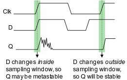
As with the basic cells, a D flip-flop or D-latch can enter a metastable state if the data and control inputs are changed at exactly the same time. In a D-latch, the data must be stable when the control input is de-asserted. In a DFF, the data input must be stable for a time immediately before and immediately after the clock edge. If the data is not stable at the clock edge, a metastable state may be clocked into the memory element. If this happens, the memory element may not be able to immediately resolve to either low voltage or high voltage, and it may oscillate for a time. Thus, when designing circuits using edge-triggered flip-flops, it is important to ensure the data input is stable for adequate time prior to the clock edge (known as the setup time), and for a time after the clock edge (known as the hold time). Setup and hold times vary between several tens of picoseconds (for designs inside single IC's) to several nanoseconds (for designs using discrete logic chips).
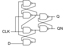
A schematic for a basic D flip-flop is shown in Fig. 4 above. Several slightly different schematics can be found in various references, but any circuit called a DFF will exhibit the same behavior.
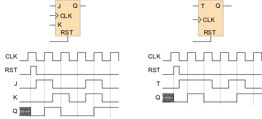
The DFF is the simplest and most useful edge-triggered memory device. Its output depends on a Data input and the clock input—at the active clock edge, the device output is driven to match the device's data input. The D-FF can be used in any application that requires a flip- flop. Over the years, other flip-flops have been designed that behave similar to, but not exactly like a DFF. One common device, called a JK flip-flop, uses two inputs to direct state changes (the J input sets the output, and the K input resets the output; if both are asserted, the output toggles between '1' and '0'). Another common device, the T flip-flop, simply toggles between '1' and '0' on each successive clock edge so long as the T input is asserted. These devices were commonly used in older digital systems (especially those built of discrete 7400 logic ICs), but they are rarely encountered in modern designs. Both JK-FF and T-FF can be easily constructed from DFFs or from first principles using basic cells. In modern digital design, and particularly in designs destined for FPGAs or other complex logic chips, these other flip-flops offer no advantages and they will not be dealt with further here. Figure 6 below illustrates JK and T flip-flops.
Important Ideas
- All useful memory devices have at least two inputs—one for the data signal to be memorized, and a timing control signal to define exactly when the Data signal should be memorized.
- The current output of a memory device is called the “present state”, and the input is called the “next state” because it will define the memory at the next assertion of the timing control input.
- Flip-flop circuits are constructed in such a way as to make them operate properly when they are part of a sequential circuit that employs a single clock.
- In a DFF, the data input must be stable for a time immediately before and immediately after the clock edge.
- A JK flip-flop uses two inputs to direct state changes (the J input sets the output, and the K input resets the output; if both are asserted, the output toggles between '1' and '0').
- The T flip-flop simply toggles between '1' and '0' on each successive clock edge so long as the T input is asserted.


沒有留言:
張貼留言