2012年10月29日 星期一

P7-10 以2x4 Deocder 完成 3x8 Decoder 適用於DE2-70

P7-10 以2x4 Deocder 完成 3x8 Decoder 適用於DE2-70

//---------------------------------------------------
// 3 to 8 decoder using a function of 2 to 4 decoders
// Filename : decod_fcn.v
//---------------------------------------------------
module decoder_3x8 (SW, LEDR, LEDG , CLOCK_27 ,KEY ,HEX0 ,HEX1 ,HEX2,HEX3 );

input  [17:0] SW; // toggle switches
input  [7:0] KEY;     // Push bottom
input  CLOCK_27; //Clock 27MHz , 50Mhz

output [17:0] LEDR; // red  LEDS   
  output [8:0] LEDG; // green LEDs
    
    output [6:0] HEX0,HEX1,HEX2,HEX3; //7-segment display
    
  
//set original program input , output 

//(Din, Y);
//input [2:0] Din;  //3-bit data input
//output [7:0] Y;   //8-bit data output

wire [2:0] Din;
wire [7:0] Y;

    assign Din =SW[2:0];
    assign LEDR[2:0]=SW[2:0];


    reg [7:0] Ytmp; // 8-bit temp register

always @(Din)
begin
Ytmp[7:4] = decod4(Din[1:0], Din[2]);
Ytmp[3:0] = decod4(Din[1:0], ~Din[2]);
end
assign Y = Ytmp;

assign LEDG[7:0]=Y;


//========================================================  
function [3:0] decod4;  // 4-bit decoder function
input [1:0] D;
input ce;     // Chip enable
if (ce == 1'b1)
begin
case (D)
2'b00 : decod4 = 4'b0001;
2'b01 : decod4 = 4'b0010;
2'b10 : decod4 = 4'b0100;
2'b11 : decod4 = 4'b1000;
default : decod4 = 4'b0000;
endcase
end
else
decod4 = 4'b0000;
   endfunction

endmodule

源自於

Binary Decoder

A Decoder is the exact opposite to that of an "Encoder" we looked at in the last tutorial. It is basically, a combinational type logic circuit that converts the binary code data at its input into one of a number of different output lines, one at a time producing an equivalent decimal code at its output. Binary Decodershave inputs of 2-bit, 3-bit or 4-bit codes depending upon the number of data input lines, and a n-bitdecoder has 2n output lines.
Therefore, if a binary decoder receives n inputs (usually grouped as a binary or Boolean number) it activates one and only one of its 2n outputs based on that input with all other outputs deactivated. A decoders output code normally has more bits than its input code and practical "binary decoder" circuits include, 2-to-4, 3-to-8 and 4-to-16 line configurations.
A Binary Decoder converts coded inputs into coded outputs, where the input and output codes are different and decoders are available to "decode" either a Binary or BCD (8421 code) input pattern to typically a Decimal output code. Commonly available BCD-to-Decimal decoders include the TTL 7442 or the CMOS 4028. An example of a 2-to-4 line decoder along with its truth table is given below. It consists of an array of four NAND gates, one of which is selected for each combination of the input signals A andB.

A 2-to-4 Binary Decoders.

Binary Decoder

Binary Decoder Truth Table

In this simple example of a 2-to-4 line binary decoder, the binary inputs A and B determine which output line from D0 to D3 is "HIGH" at logic level "1" while the remaining outputs are held "LOW" at logic "0" so only one output can be active (HIGH) at any one time. Therefore, whichever output line is "HIGH" identifies the binary code present at the input, in other words it "de-codes" the binary input and these types of binary decoders are commonly used as Address Decoders in microprocessor memory applications.
3-to-8 Binary Decoder
74LS138 Binary Decoder
Some binary decoders have an additional input labelled "Enable" that controls the outputs from the device. This allows the decoders outputs to be turned "ON" or "OFF" and we can see that the logic diagram of the basic decoder is identical to that of the basic demultiplexer.
Then, we can say that a binary decoder is a demultiplexer with an additional data line that is used to enable the decoder. An alternative way of looking at the decoder circuit is to regard inputs A, B and C as address signals. Each combination of A, B or C defines a unique address which can access a location having that address.
Sometimes it is required to have a Binary Decoder with a number of outputs greater than is available, or if we only have small devices available, we can combine multiple decoders together to form larger decoder networks as shown. Here a much larger 4-to-16 line binary decoder has been implemented using two smaller 3-to-8 decoders.

A 4-to-16 Binary Decoder Configuration.

Binary Decoder
Inputs A, B, C are used to select which output on either decoder will be at logic "1" (HIGH) and input Dis used with the enable input to select which encoder either the first or second will output the "1".

Memory Address Decoder.

Binary Decoders are most often used in more complex digital systems to access a particular memory location based on an "address" produced by a computing device. In modern microprocessor systems the amount of memory required can be quite high and is generally more than one single memory chip alone. One method of overcoming this problem is to connect lots of individual memory chips together and to read the data on a common "Data Bus". In order to prevent the data being "read" from each memory chip at the same time, each memory chip is selected individually one at time and this process is known as Address Decoding.
In this application, the address represents the coded data input, and the outputs are the particular memory element select signals. Each memory chip has an input called Chip Select or CS which is used by the MPU to select the appropriate memory chip and a logic "1" on this input selects the device and a logic "0" on the input de-selects it. By selecting or de-selecting each chip, allows us to select the correct memory device for a particular address and when we specify a particular memory address, the corresponding memory location exists ONLY in one of the chips.
For example, Lets assume we have a very simple microprocessor system with only 1Kb of RAM memory and 10 address lines. The memory consists of 128x8-bit (128x8 = 1024 bytes) devices and for 1Kb we will need 8 individual memory devices but in order to select the correct memory chip we will also require a 3-to-8 line binary decoder as shown below.

Memory Address Decoding.

Memory Address Decoder
The binary decoder requires 3 address lines, (A0 to A2) to select each one of the 8 chips (the lower part of the address), while the remaining 7 address lines (A3 to A9) select the correct memory location on that chip (the upper part of the address). Having selected a memory location using the address bus, the information at the particular internal memory location is sent to the "Data Bus" for use by the microprocessor. This is of course a simple example but the principals remain the same for all types of memory chips or modules.
Binary Decoders are very useful devices for converting one digital format to another, such as binary or BCD type data into decimal or octal etc and commonly available decoder IC's are the TTL 74LS138 3-to-8 line binary decoder or the 74ALS154 4-to-16 line decoder. They are also very useful for interfacing to 7-segment displays such as the TTL 74LS47 which we will look at in the next tutorial.

P7-7以1x2 DeMux完成1X4 DeMux 適用於DE2-70

P7-7以1x2 DeMux完成1X4 DeMux 適用於DE2-70


//--------------------------------------------------
// 1 to 4 demultiplexer using 1 to 2 demultiplexers
// with function call
// Filenale : dmux14_fcn.v
//--------------------------------------------------

module demux_1x4 (SW, LEDR, LEDG , CLOCK_27 ,KEY ,HEX0 ,HEX1 ,HEX2,HEX3 );

input  [17:0] SW; // toggle switches
input  [7:0] KEY;     // Push bottom
input  CLOCK_27; //Clock 27MHz , 50Mhz

output [17:0] LEDR; // red  LEDS   
  output [8:0] LEDG; // green LEDs
    
    output [6:0] HEX0,HEX1,HEX2,HEX3; //7-segment display
    
  
//set original program input , output 


//dmux14_fcn(Din, S, Y);
//input Din;      // Data input
//input [1:0] S;  // 2-bit select line
//output [3:0] Y; // 4-bit output

    wire Din;
    wire [1:0] S;
reg [3:0] Y;  
reg [1:0] X;
  

assign Din=SW[17];
assign  S[1:0]=SW[1:0];
assign  LEDR[17]=SW[17];
assign  LEDR[1:0]=SW[1:0];


always @(Din or S)
begin
X = DEMUL2(S[1], Din);        // The first 1 to 2 demultiplexer
Y[1:0] = DEMUL2(S[0], X[0]);  // The second 1 to 2 demultiplexer
Y[3:2] = DEMUL2(S[0], X[1]);  // The third 1 to 2 demultiplexer
end

   assign LEDG[3:0]=Y; 

//=====================================================

function [1:0] DEMUL2; // Function of 1 to 2 demultiplexer 
input S;
input D;
case(S)
1'b0 : DEMUL2 = {1'b0, D};
1'b1 : DEMUL2 = {D, 1'b0};
default : DEMUL2 = {1'b0, 1'b0};
endcase
endfunction

endmodule


源自於
http://www.electronics-tutorials.ws/combination/comb_3.html

The Demultiplexer

The data distributor, known more commonly as a Demultiplexer or "Demux", is the exact opposite of theMultiplexer we saw in the previous tutorial. The demultiplexer takes one single input data line and then switches it to any one of a number of individual output lines one at a time. The demultiplexerconverts a serial data signal at the input to a parallel data at its output lines as shown below.

1-to-4 Channel De-multiplexer

Demultiplexer Circuit

AddressingInput
Selected
ba
00A
01B
10C
11D
The Boolean expression for this 1-to-4 Demultiplexer above with outputs A to D and data select lines a, b is given as:
F = ab A + abB +  abC + abD
The function of the Demultiplexer is to switch one common data input line to any one of the 4 output data lines A to D in our example above. As with the multiplexer the individual solid state switches are selected by the binary input address code on the output select pins "a" and "b" and by adding more address line inputs it is possible to switch more outputs giving a 1-to-2n data line outputs.
Some standard demultiplexer IC´s also have an additional "enable output" pin which disables or prevents the input from being passed to the selected output. Also some have latches built into their outputs to maintain the output logic level after the address inputs have been changed. However, in standard decoder type circuits the address input will determine which single data output will have the same value as the data input with all other data outputs having the value of logic "0".
The implementation of the Boolean expression above using individual logic gates would require the use of six individual gates consisting of AND and NOT gates as shown.

4 Channel Demultiplexer using Logic Gates

4 Channel Demultiplexer using Logic Gates

The symbol used in logic diagrams to identify a demultiplexer is as follows.

The Demultiplexer Symbol

Deultiplexer Symbol
Standard Demultiplexer IC packages available are the TTL 74LS138 1 to 8-output demultiplexer, the TTL 74LS139 Dual 1-to-4 output demultiplexer or the CMOS CD4514 1-to-16 output demultiplexer. Another type of demultiplexer is the 24-pin, 74LS154 which is a 4-bit to 16-line demultiplexer/decoder. Here the individual output positions are selected using a 4-bit binary coded input. Like multiplexers, demultiplexers can also be cascaded together to form higher order demultiplexers.
Unlike multiplexers which convert data from a single data line to multiple lines and demultiplexers which convert multiple lines to a single data line, there are devices available which convert data to and from multiple lines and in the next tutorial about combinational logic devices, we will look at Encoderswhich convert multiple input lines into multiple output lines, converting the data from one form to another.

P7-5 以8bit Even Parity 產生16bit Even Parity Checker 適用於DE2-70


P7-5 以8bit Even Parity 產生16bit Even Parity Checker 
適用於DE2-70


//-----------------------------------------------
// 16-bit even-parity generator using two 8-bit 
// even-parity generators
// Filename : even_parity_16.v
//-----------------------------------------------
module even_parity (SW, LEDR, LEDG , CLOCK_27 ,KEY ,HEX0 ,HEX1 ,HEX2,HEX3 );

input  [17:0] SW; // toggle switches
input  [7:0] KEY;     // Push bottom
input  CLOCK_27; //Clock 27MHz , 50Mhz
output [17:0] LEDR; // red  LEDS   
  output [8:0] LEDG; // green LEDs
    
    output [6:0] HEX0,HEX1,HEX2,HEX3; //7-segment display
    
  
//set original program input , output 
//(Din, Pout);
//input [15:0] Din;
//output Pout;
  
    wire [15:0] Din;
reg [7:0] High_byte; // Hight byte of input data
reg [7:0] Low_byte;  // Low byte of input data
reg High, Low;       // Parities of high and low byte
reg Pout;        // Parity output

assign Din=SW[15:0];

always @(Din)
begin
High_byte = Din[15:8];
Low_byte = Din[7:0];
High = even8(High_byte);
Low = even8(Low_byte);
Pout = High ^ Low; // Bitwise xor
end

    assign LEDG[0]=Pout;
    
//=====================================================
function even8;
input [7:0] I;
begin 
even8 = ^ I; // reduction xor operation
end
endfunction

endmodule


2012年10月28日 星期日

P6-76 4bit BCD Adder 適用於DE2-70


P6-76 4bit BCD Adder 適用於DE2-70 

BCD加法器
BCD加法運算原則:
  1. 將二個BCD碼先以4位元二進位數加法運算。
  2. 運算後四位元總和小於或等於9(1001B),且無進位產生,則此”和”為有效BCD值。
  3. 運算後四位元總和大於9(1001B)或有進位產生,則必須將”和”再加上6(011B),才為有效BCD值。
  4. 將上述步驟產生三進位加至下一位數。   
依上述原則可得一真值表
P7-1.gif (1367 bytes)輸出Y=0表示有效BCD碼,不加6。
輸出
Y=1表示需要加6調整。Y=B3B2+B3B1+C4
   =B3(B2+B1)+C4
 

若要以二進加法器做BCD碼的加法,其和大於9的數必須加6來修正,至於電路方面就必須有個大於9的檢查電路,能檢知當加法器的和大於9時自動加6,如例6.4-2中的情形。另一種情形如例6.4-3,BCD碼相加的和(0001)並未大於9,但是產生進位後實際的二進值為10001(17),也是大於9,所以圖6.4-1中須要加6的修正的包括主要四位元二進加法器的和S3 S2 S1 S0大於9以及進位CO等於1之時,至於大於9的電路設計可以參考前章中的例5.3-3。

6-1-4.gif (6644 bytes)

//------------------------------------
//4-bit BCD adder
//Filename : BCDadder4.v
//------------------------------------
module _4bit_BCD_Adder(SW, LEDR, LEDG , CLOCK_27 ,KEY ,HEX0 ,HEX1 ,HEX2,HEX3 );

input  [17:0] SW; // toggle switches
input  [7:0] KEY;     // Push bottom
input  CLOCK_27; //Clock 27MHz , 50Mhz

output [17:0] LEDR; // red  LEDS   
  output [8:0] LEDG; // green LEDs
    
    output [6:0] HEX0,HEX1,HEX2,HEX3; //7-segment display
    
  
//set original program input , output 
  
  
//(S, Cout, Cin, A, B);
//output [3:0] S; //Sumation output
//output Cout;    //Carry out
//input Cin;      //Carry in
//input [3:0] A, B;//Input data
  
    wire Cin;      //Carry in
    wire [3:0] A, B;//Input data
    wire [3:0] S; //Sumation output
    wire Cout;    //Carry out
    
reg [3:0] gt9=4'b101;

    wire [7:0] segout0;   //HEX 0
    wire [7:0] segout1;   //HEX 1
    
    assign  A=SW[3:0] ;
    assign  B=SW[7:4] ;
    assign  Cin=SW[17];
    
    reg [3:0] A_tmp,B_tmp;
  
wire [3:0] S_tmp;
wire C4;
reg [3:0] B_mod;
reg F;

    always @ ( A or B )
begin
if (A<10)
  A_tmp = A;   //若是>9 則為9
else
  A_tmp =4'b1001;

if (B<10)
  B_tmp = B;  //若是>9 則為9
else
  B_tmp =4'b1001;
end


//4-bit binary adder
adder4 BINADD(
            .S(S_tmp),
            .Cout(C4),
            .Cin(Cin),
            .A(A_tmp),
            .B(B_tmp)
           );

//Modify binary code with '0110'
adder4 MODADD(
            .S(S),
            .Cout(),
            .Cin(1'b0),
            .A(S_tmp),
            .B(B_mod)
           );

always @ (Cin or A or B or C4 or S_tmp)
begin
//F=C4+S3(S2+S1)
F = (C4 | (S_tmp[3] & (S_tmp[2] | S_tmp[1])));
B_mod = {1'b0, F, F, 1'b0}; //Modified code
end
assign Cout = F;


_7seg UUT0(.hex((S)),
               .seg(segout0));
    
    _7seg UUT1(.hex({3'b0,Cout}),
               .seg(segout1));
    
           
    assign HEX0=segout0[6:0];
    assign HEX1=segout1[6:0];
   
endmodule


//----------------------
//4-bit unsigned adder
//Filename : adder4.v
//----------------------                                                                                                                                                                                                                   
module adder4(S, Cout, A, B, Cin);
output [3:0] S;   //4-bit sum
output Cout;   //Carry out
input [3:0] A, B; //Inputs
input Cin;   //Carry in

//Assign the sum of (A+B+Cin) to Cout and Sum
assign {Cout, S} = A + B + Cin;

endmodule


//-----------------------------------------
//Common-cathod seven segment display
//using case.....endcase statement
//Filename : sevenseg_case.v
//----------------------------------------- 
module _7seg(hex , seg);
    input  [3:0] hex;
    output [7:0] seg;
    reg    [7:0] seg;


// segment encoding
//      0
//     ---  
//  5 |   | 1
//     ---   <- 6
//  4 |   | 2
//     ---
//      3
always @(hex)
begin
case (hex)
       // Dot point is always disable
       4'b0001 : seg = 8'b11111001;   //1 = F9H
       4'b0010 : seg = 8'b10100100;   //2 = A4H
       4'b0011 : seg = 8'b10110000;   //3 = B0H
       4'b0100 : seg = 8'b10011001;   //4 = 99H
       4'b0101 : seg = 8'b10010010;   //5 = 92H
       4'b0110 : seg = 8'b10000010;   //6 = 82H
       4'b0111 : seg = 8'b11111000;   //7 = F8H
       4'b1000 : seg = 8'b10000000;   //8 = 80H
       4'b1001 : seg = 8'b10010000;   //9 = 90H
       4'b1010 : seg = 8'b10001000;   //A = 88H
       4'b1011 : seg = 8'b10000011;   //b = 83H
       4'b1100 : seg = 8'b11000110;   //C = C6H
       4'b1101 : seg = 8'b10100001;   //d = A1H
       4'b1110 : seg = 8'b10000110;   //E = 86H
       4'b1111 : seg = 8'b10001110;   //F = 8EH
       default : seg = 8'b11000000;   //0 = C0H
     endcase
   end
   
endmodule


P6-70 2 digit BCD Counter 00-99 適用於DE2-70 (SW0 往上撥 才能計數 , 往下撥 Reset)

P6-70 2 digit BCD Counter 00-99 適用於DE2-70  (SW0 往上撥 才能計數 ,  往下撥 Reset)

源自於http://www.electronics-tutorials.ws/counter/count_2.html

Asynchronous Counter

In the previous tutorial we saw that an Asynchronous counter can have 2n-1 possible counting states e.g. MOD-16 for a 4-bit counter, (0-15) making it ideal for use in Frequency Division. But it is also possible to use the basic asynchronous counter to construct special counters with counting states less than their maximum output number by forcing the counter to reset itself to zero at a pre-determined value producing a type of asynchronous counter that has truncated sequences. Then an n-bit counter that counts up to its maximum modulus (2n) is called a full sequence counter and a n-bit counter whose modulus is less than the maximum possible is called a truncated counter.
But why would we want to create an asynchronous truncated counter that is not a MOD-4, MOD-8, or some other modulus that is equal to the power of two. The answer is that we can by using combinational logic to take advantage of the asynchronous inputs on the flip-flop. If we take the modulo-16 asynchronous counter and modified it with additional logic gates it can be made to give a decade (divide-by-10) counter output for use in standard decimal counting and arithmetic circuits.
Such counters are generally referred to as Decade Counters. A decade counter requires resetting to zero when the output count reaches the decimal value of 10, ie. when DCBA = 1010 and to do this we need to feed this condition back to the reset input. A counter with a count sequence from binary "0000" (BCD = "0") through to "1001" (BCD = "9") is generally referred to as a BCD binary-coded-decimal counter because its ten state sequence is that of a BCD code but binary decade counters are more common.

Asynchronous Decade Counter

Asynchronous Decade Counter
This type of asynchronous counter counts upwards on each leading edge of the input clock signal starting from "0000" until it reaches an output "1010" (decimal 10). Both outputs QB and QD are now equal to logic "1" and the output from the NAND gate changes state from logic "1" to a logic "0" level and whose output is also connected to the CLEAR (CLR) inputs of all the J-K Flip-flops.
This signal causes all of the Q outputs to be reset back to binary "0000" on the count of 10. Once QB andQD are both equal to logic "0" the output of the NAND gate returns back to a logic level "1" and the counter restarts again from "0000". We now have a decade or Modulo-10 counter.

Decade Counter Truth Table

Clock
Count
Output bit PatternDecimal
Value
QDQCQBQA
100000
200011
300102
400113
501004
601015
701106
801117
910008
1010019
11Counter Resets its Outputs back to Zero

Decade Counter Timing Diagram

Asynchronous Decade Counter Timing

Using the same idea of truncating counter output sequences, the above circuit could easily be adapted to other counting cycles be simply changing the connections to the AND gate. For example, a scale-of-twelve (modulo-12) can easily be made by simply taking the inputs to the AND gate from the outputs at "QC" and "QD", noting that the binary equivalent of 12 is "1100" and that output "QA" is the least significant bit (LSB).
Since the maximum modulus that can be implemented with n flip-flops is 2n, this means that when you are designing truncated asynchronous counters you should determine the lowest power of two that is greater than or equal to your desired modulus. For example, lets say you wish to count from 0 to 39, or mod-40. Then the highest number of flip-flops required would be six, n = 6 giving a maximum MOD of 64 as five flip-flops would only equal MOD-32.
divide-by-128 CounterNow suppose we wanted to build a "divide-by-128" counter for frequency division we would need to cascade seven flip-flops since 128 = 27. Using dual flip-flops such as the 74LS74 we would still need four IC's to complete the circuit.
One easy alternative method would be to use two TTL 7493's as 4-bit ripple counter/dividers. Since 128 = 16 x 8, one 7493 could be configured as a "divide-by-16" counter and the other as a "divide-by-8" counter. The two IC's would be cascaded together to form a "divide-by-128" frequency divider as shown.
Of course standard IC asynchronous counters are available such as the TTL 74LS90 programmable ripple counter/divider which can be configured as a divide-by-2, divide-by-5 or any combination of both. The 74LS390 is a very flexible dual decade driver IC with a large number of "divide-by" combinations available ranging form divide-by-2, 4, 5, 10, 20, 25, 50, and 100.


//top-level module for 2-digit BCD counter 00-->99
// 
module _2digit_BCD_count(SW, LEDR, LEDG , CLOCK_27 ,KEY ,HEX0 ,HEX1 ,HEX2,HEX3 );

input  [17:0] SW; // toggle switches
input  [7:0] KEY;     // Push bottom
input  CLOCK_27; //Clock 27MHz , 50Mhz

output [17:0] LEDR; // red  LEDS   
  output [8:0] LEDG; // green LEDs
    
    output [6:0] HEX0,HEX1,HEX2,HEX3; //7-segment display
    
  
//set original program input , output 
  
//(clk,reset,one_out,ten_out);
//input clk,reset;
//output [3:0] one_out,ten_out;
    wire clk,reset;
    //reg [3:0] one_out,ten_out;
    
  
    wire [7:0] segout0;   //HEX 0
    wire [7:0] segout1;   //HEX 1
    
    assign  reset=SW[0] ;
    assign  clk =KEY[0];  
    
    
wire nreset,ones_en,tens_en,tc_ones;  //tc_ones --> 1's carry out
wire [3:0] one_out , ten_out;
  
  
// module cnt_10(ce,clk, clr,tc,qout);
cnt_10 _1s (.ce(ones_en),
             .clk(clk),
             .clr(nreset),
             .tc(tc_ones),    //1's carry out
.qout(one_out)
);
  
cnt_10 _10s (.ce(tens_en),
             .clk(clk),
             .clr(nreset),
             .tc(), //10's carry out  ignore   
             .qout(ten_out)
             );
             
assign tens_en=tc_ones;
assign ones_en =1'b1;
assign nreset=~reset;


_7seg UUT0(.hex((one_out)),
               .seg(segout0));
    
    _7seg UUT1(.hex((ten_out)),
               .seg(segout1));


    assign HEX0=segout0[6:0];
    assign HEX1=segout1[6:0];
    

endmodule

//====================================


//BCD counter counts 0 to 9 and then rolls over
module cnt_10(ce,clk,clr,tc,qout);
  input ce,clk,clr;
  output tc;  //carry out
  output [3:0] qout;
  
  reg [3:0] count;
  
  always @(posedge clk or posedge clr)
  begin
    if (clr)  //clear 
        count <=4'b0;
    else 

if (ce) 
      if (count==4'h9)
          count <=4'h0;
      else    
          count <= count +1;
  end        
  
  assign qout = count ;
  assign tc=(count==4'h9);   //if count=9 then carry out=1

endmodule

//======================================


//-----------------------------------------
//Common-cathod seven segment display
//using case.....endcase statement
//Filename : sevenseg_case.v
//----------------------------------------- 
module _7seg(hex , seg);

    input  [3:0] hex;
    output [7:0] seg;
    reg    [7:0] seg;


// segment encoding
//      0
//     ---  
//  5 |   | 1
//     ---   <- 6
//  4 |   | 2
//     ---
//      3

always @(hex)
begin
case (hex)
       // Dot point is always disable
       4'b0001 : seg = 8'b11111001;   //1 = F9H
       4'b0010 : seg = 8'b10100100;   //2 = A4H
       4'b0011 : seg = 8'b10110000;   //3 = B0H
       4'b0100 : seg = 8'b10011001;   //4 = 99H
       4'b0101 : seg = 8'b10010010;   //5 = 92H
       4'b0110 : seg = 8'b10000010;   //6 = 82H
       4'b0111 : seg = 8'b11111000;   //7 = F8H
       4'b1000 : seg = 8'b10000000;   //8 = 80H
       4'b1001 : seg = 8'b10010000;   //9 = 90H
       4'b1010 : seg = 8'b10001000;   //A = 88H
       4'b1011 : seg = 8'b10000011;   //b = 83H
       4'b1100 : seg = 8'b11000110;   //C = C6H
       4'b1101 : seg = 8'b10100001;   //d = A1H
       4'b1110 : seg = 8'b10000110;   //E = 86H
       4'b1111 : seg = 8'b10001110;   //F = 8EH
       default : seg = 8'b11000000;   //0 = C0H
     endcase
   end
   

endmodule


P6-63 repeat loop 計數8bit 中1's數量

P6-63 repeat loop 計數8bit 中1's數量


Repeat Loop

        
        module comply;
          int count;
        // counting down from 128

        initial begin
          count = 128;
          repeat (count) begin
             $display("%d seconds to comply", count);
             count = count - 1;
          end
        end

        endmodule


//-------------------------------
//Count one bits in a 8-bit word
//using repeat loop
//Filename : repeat_1s.v
//-------------------------------
module _1s_count (SW, LEDR, LEDG , CLOCK_27 ,KEY ,HEX0 ,HEX1 ,HEX2,HEX3 );

input  [17:0] SW; // toggle switches
input  [7:0] KEY;     // Push bottom
input  CLOCK_27; //Clock 27MHz , 50Mhz

output [17:0] LEDR; // red  LEDS   
  output [8:0] LEDG; // green LEDs
    
    output [6:0] HEX0,HEX1,HEX2,HEX3; //7-segment display
    
  
//set original program input , output 
parameter length = 8;          //Data length
    
// (ones, Din);

reg  [3:0] ones;  //Output the number of ones
wire [length-1:0] Din; //8-bit data input

reg [length-1:0] tmpr;
reg [3:0] Cout;

  
    wire [7:0] segout1;   //HEX 0
    
    assign  Din=SW[7:0] ;  
    
    
    always @ (Din)
begin
Cout = 4'b0000;
tmpr = Din;

repeat (length)
begin
if (tmpr[0]) Cout = Cout + 4'b0001;
tmpr = tmpr >> 1;    //shift right 
end
ones = Cout;
end

assign LEDG[3:0]=Cout;


_7seg UUT1(.hex((Cout)),
               .seg(segout1));
       
    assign HEX0=segout1[6:0];

endmodule


//-----------------------------------------
//Common-cathod seven segment display
//using case.....endcase statement
//Filename : sevenseg_case.v
//----------------------------------------- 
module _7seg(hex , seg);

    input  [3:0] hex;
    output [7:0] seg;
    reg    [7:0] seg;


// segment encoding
//      0
//     ---  
//  5 |   | 1
//     ---   <- 6
//  4 |   | 2
//     ---
//      3

always @(hex)
begin
case (hex)
       // Dot point is always disable
       4'b0001 : seg = 8'b11111001;   //1 = F9H
       4'b0010 : seg = 8'b10100100;   //2 = A4H
       4'b0011 : seg = 8'b10110000;   //3 = B0H
       4'b0100 : seg = 8'b10011001;   //4 = 99H
       4'b0101 : seg = 8'b10010010;   //5 = 92H
       4'b0110 : seg = 8'b10000010;   //6 = 82H
       4'b0111 : seg = 8'b11111000;   //7 = F8H
       4'b1000 : seg = 8'b10000000;   //8 = 80H
       4'b1001 : seg = 8'b10010000;   //9 = 90H
       4'b1010 : seg = 8'b10001000;   //A = 88H
       4'b1011 : seg = 8'b10000011;   //b = 83H
       4'b1100 : seg = 8'b11000110;   //C = C6H
       4'b1101 : seg = 8'b10100001;   //d = A1H
       4'b1110 : seg = 8'b10000110;   //E = 86H
       4'b1111 : seg = 8'b10001110;   //F = 8EH
       default : seg = 8'b11000000;   //0 = C0H
     endcase
   end
   

endmodule

P6-58 8bit Gray change into Binary code適用於DE2-70

P6-58 8bit Gray change into Binary code適用於DE2-70


源自於http://verticalhorizons.in/binary-to-gray-code-converter-gray-to-binary-code-converter/

Binary To Gray Code Converter – Gray to Binary Code Converter


The conversion between gray to binary and binary to gray is very common in digital systems. In one of our previous post we explained what are gray codes and how to convert from binary to gray and gray to binary. This post focus on implementing code converter using logic gates.

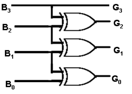
Binary to Gray Code Converter

Gray code equivalent of the given binary number is computed as follows:
g3 = b3
g2 = b3 ⊕ b2
g1 = b2 ⊕ b1
g0 = b1 ⊕ b0
A binary to gray code converter can be implemented using XORgates. For n input, n-1 gates are required. As shown in the image below for 4 inputs, 3 XOR gates are used:

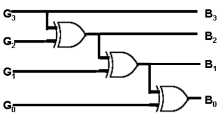
Gray to Binary Code Converter

Binary code equivalent of the given gray number is computed as follows:
b3 = g3
b2 = b3 ⊕ g2
b1 = b2 ⊕ g1
b0 = b1 ⊕ g0
A gray to binary code converter can be implemented using XORgates. For n input, n-1 gates are required. As shown in the image below for 4 inputs, 3 XOR gates are used:

//--------------------------------------
//Convert 8-bit Gray code to binary code 
//using for loop
//filename : gra2bin.v
//--------------------------------------
module gray2bin(SW, LEDR, LEDG , CLOCK_27 ,KEY ,HEX0 ,HEX1 ,HEX2,HEX3 );

input  [17:0] SW; // toggle switches
input  [7:0] KEY;     // Push bottom
input  CLOCK_27; //Clock 27MHz , 50Mhz
output [17:0] LEDR; // red  LEDS   
  output [7:0] LEDG; // green LEDs
    
    output [6:0] HEX0,HEX1,HEX2,HEX3; //7-segment display
    parameter length = 8;       //8-bit length
  
//set original program input , output 

//bin2gra(Gry, Bin);
//output [length-1:0] Gry;    //Gray code putput
//input [length-1:0] Bin;     //Binary input
reg  [length-1:0] Bin;
wire [length-1:0] Gry;
    
        
    //mapping to hardware 
    assign LEDR = SW;
    assign Gry=SW[7:0];
    

integer i;


always @ (Gry)
begin
Bin[length-1]=Gry[length-1]; 
for (i=length-2; i>=0; i = i-1)
Bin[i]=Bin[i+1] ^ Gry[i];
end
    
    assign LEDG[7:0]=Bin;

endmodule


  清除項目編譯快取 執行 flutter clean 重新取得套件依賴 執行 flutter pub get 完整重新編譯並執行 flutter run 1. 新增專案套件 (pubspec.yaml) 在 Flutter 專案根目錄下的 pubspec.yaml 中,新增 ...